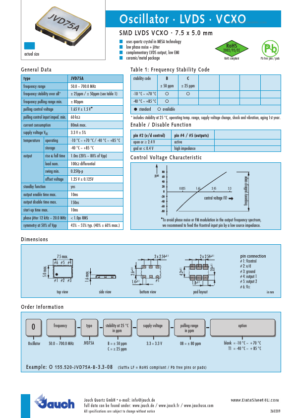
JVD75A
JVD75A is SMD LVDS VCXO manufactured by Jauch Quartz Gmbh.
Oscillator
- LVDS
- VCXO
SMD LVDS VCXO
- 7.5 x 5.0 mm actual size
- -
- - uses quartz crystal in MESA technology low phase noise + jitter plementary LVDS output, low EMI ceramic/metal package
..
2002/95/EC
Ro HS pliant Pb free: pins / pads
Ro HS
General Data type frequency range frequency stability over all- frequency pulling range min. pulling control voltage pulling control input imped. min. current consumption supply voltage VDC temperature operating storage output rise & fall time load nom. swing min. offset voltage standby function output enable time max. output disable time max. start-up time max. phase jitter 12 k Hz ~ 20.0 MHz symmetry at 50% of Vpp JVD75A 50.0 ~ 700.0 MHz ± 25ppm / ± 50ppm (see table 1) ± 80ppm 1.65 V ± 1.5 V 60 kΩ 80m A max. 3.3 V ± 5% -10 °C ~ +70 °C / -40 °C ~ +85 °C -40 °C ~ +85 °C 1.0ns (20% ~ 80% of Vpp) 100Ω differential 0.35Vp-p 1.25 V ± 0.125V yes 10ms 150ns 10ms < 1.0ps RMS 45% ~ 55% typ. (40% ± 60% max.)
- Table 1: Frequency Stability Code stability code B ± 50 ppm -10 °C ~ +70 °C -40 °C ~ +85 °C O O O available C ± 25 ppm O
- standard
- includes stability at 25 °C, operating temp. range, supply voltage change, shock and vibration, aging 1st year.
Enable / Disable Function pin #2 (e/d control) open or ≥ 2.4 V gnd or ≤ 0.4 V pin #4 / #5 (outputs) active high impedance
Control Voltage Characteristic ppm
3.3 control voltage (V)
- To avoid phase noise or FM modulation in the output frequency spectrum, we remend to feed the Vcontrol input pin by a low source impedance.
Dimensions
7.5 max. #6 #5 #4 5.0 max.
2 x 2.54
2 x 2.54
#1 #2 #3
#1
0.1 pin connection # 1: Vcontrol # 2: e/d # 3: ground # 4: output 1 # 5: output 2 # 6: VCC in mm
1.6 max. top view side view
2.6 bottom view
4.2 pad layout
Order...