Datasheet Summary
SEMICONDUCTOR
TECHNICAL DATA
GENERAL PURPOSE APPLICATION. SWITCHING APPLICATION.
Features
ᴌplementary to BCW31/32
MAXIMUM RATING (Ta=25ᴱ)
CHARACTERISTIC
SYMBOL RATING
Collector-Base Voltage
VCBO
-30
Collector-Emitter Voltage
VCEO
-20
Emitter-Base Voltage
VEBO
-5
Collector Current
IC -100
Collector Power Dissipation
- 350
Junction Temperature
Tj 150
Storage Temperature Range
Tstg -65ᴕ150
- : Package Mounted On 99.9% Alumina 10ᴧ8ᴧ0.6mm.
UNIT V V V mA mW ᴱ ᴱ
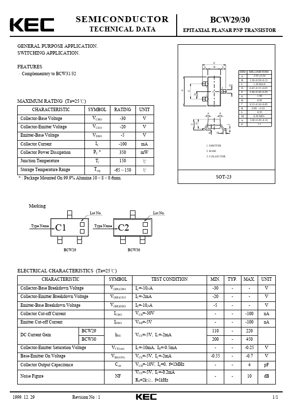
BCW29/30
EPITAXIAL PLANAR PNP TRANSISTOR
E L...