The following content is an automatically extracted verbatim text
from the original manufacturer datasheet and is provided for reference purposes only.
View original datasheet text
www.DataSheet4U.com
SEMICONDUCTOR
TECHNICAL DATA
KHB019N20P1/F1/F2
N CHANNEL MOS FIELD EFFECT TRANSISTOR
General Description
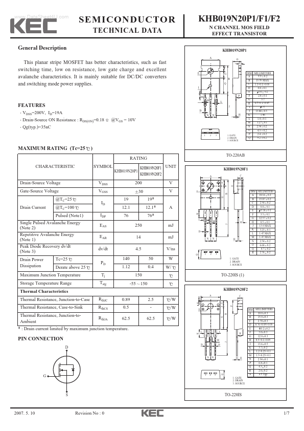
A
KHB019N20P1
O C F E G B Q I K M L J D N N H P
DIM MILLIMETERS _ 0.2 9.9 + A B C D E F G H I J K L M N O
1 2 3
This planar stripe MOSFET has better characteristics, such as fast switching time, low on resistance, low gate charge and excellent avalanche characteristics. It is mainly suitable for DC/DC converters and switching mode power supplies.
FEATURES
VDSS=200V, ID=19A Drain-Source ON Resistance : RDS(ON)=0.18 Qg(typ.)=35nC @VGS = 10V
15.95 MAX 1.3+0.1/-0.05 _ 0.1 0.8 + _ 0.2 3.6 + _ 0.1 2.8 + 3.7 0.5+0.1/-0.05 1.5 _ 0.3 13.08 + 1.46 _ 0.1 1.4 + _ 0.1 1.27 + _ 0.2 2.54 + _ 4.5 + 0.2 _ 0.2 2.4 + _ 0.2 9.2 +
1. GATE 2. DRAIN 3.