KTX212U
KTX212U is EPITAXIAL PLANAR NPN TRANSISTOR manufactured by KEC.
SEMICONDUCTOR
TECHNICAL DATA
SWITCHING APPLICATION. INTERFACE CIRCUIT AND DRIVER CIRCUIT APPLICATION.
Features
Including two devices in US6. (Ultra Super mini type with 6 leads.) With Built-in bias resistors. Simplify circuit design. Reduce a quantity of parts and manufacturing process.
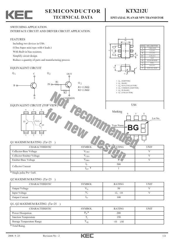
EQUIVALENT CIRCUIT
Q1 C
Q2
R1 IN
Q2 R1=2.2KΩ
R2=2.2KΩ
R2
E MON
EQUIVALENT CIRCUIT (TOP VIEW)
65 4
Q1 Q2
12 3
Q1 MAXIMUM RATING (Ta=25 ) CHARACTERISTIC
Collector-Base Voltage Collector-Emitter Voltage Emitter-Base Voltage
Collector Current
- Single pulse Pw=1m S.
Q2 MAXIMUM RATING (Ta=25 ) CHARACTERISTIC
Output Voltage Input Voltage Output Current
Q1, Q2 MAXIMUM RATING (Ta=25 ) CHARACTERISTIC
Power Dissipation Junction Temperature Storage Temperature Range
- Total Raing.
2008. 9. 23
Revision No : 2
SYMBOL VCBO VCEO VEBO IC ICP
- SYMBOL VO VI...