DESCRIPTION
These devices are well suited for high efficiency switched mode power supplies, active power factor correction based on half bridge topology. 2. FEATURES
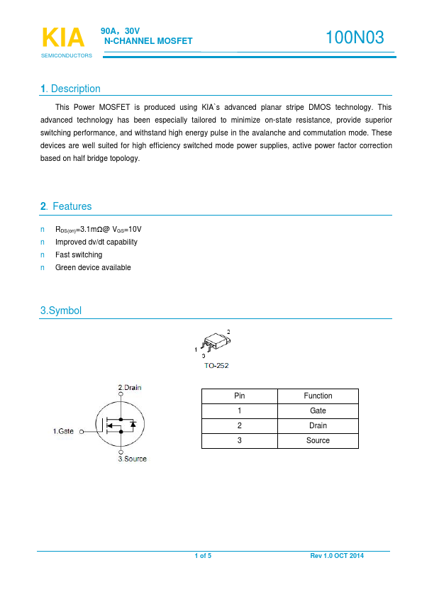
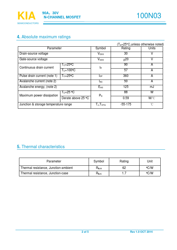
n RDS(on)=3.1mΩ@ VGS=10V n Improved dv/dt capability n Fast switching n Green device available 3.Symbol Pin Function 1 Gate 2 Drain 3 Source 1 of 5 Rev 1.0 OCT 2014 KIA 90A,30V N-CHANNEL MOSFET SEMICONDUCTORS S 4. Absolute maximum ratings Parameter Drain-source voltage Gate-source voltage Continuous drain current Pulse drain current (note 1) TC=25ºC TC=100ºC TC=25ºC Avalanche current (note 2) Avalanche energy, (note 2) TC=25 ºC Maximum power dissipation Derate above 25 ºC Junction & storage temperature range Symbol VDSS VGSS ID IDP IAS EAS PD TJ,TSTG 100N03 (TA=25°C,unless otherwise noted) Rating Units 30 V +20 V 90 A 57 A 360 A 50 A 125 mJ 88 W 0.59 W/℃ -55-175 ℃ 5. Thermal characteristics Parameter Thermal resistance, Junction-ambient Thermal resistance, Junction-case Symbol RθJA RθJC Rating 62 1.7 Unit ºC/W ºC/W 2 of 5 Rev 1.0 OCT 2014 KIA 90A,30V N-CHANNEL MOSFET 100N03 SEMICONDUCTORS 6S . KIA