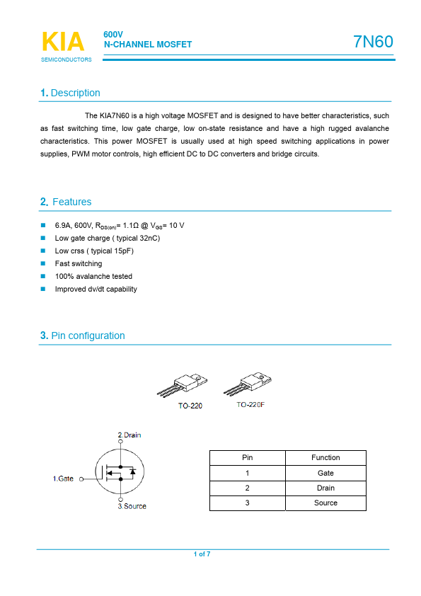
DESCRIPTION
2. FEATURES
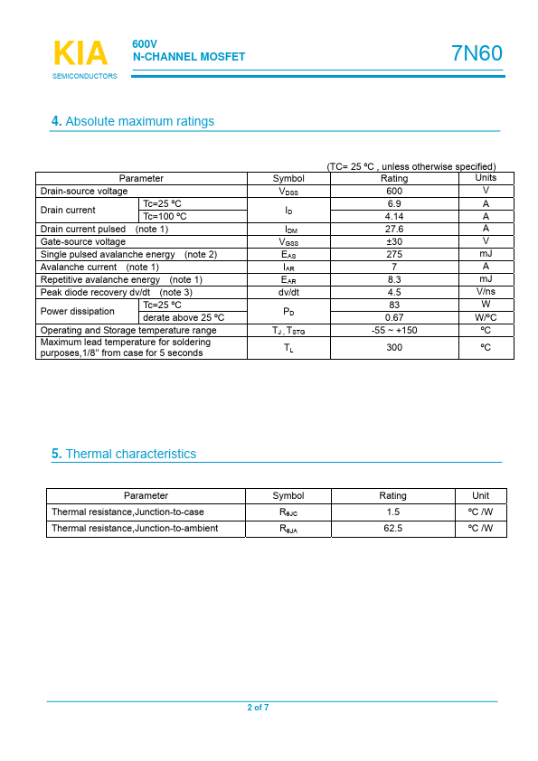
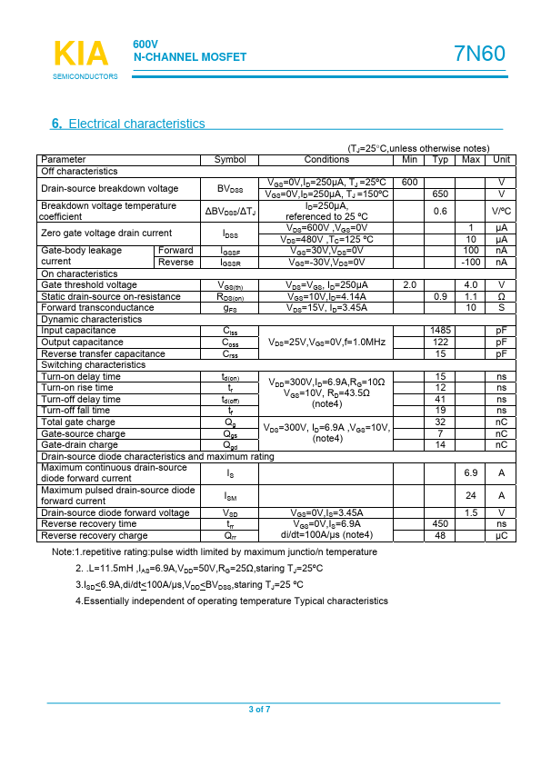
6.9A, 600V, RDS(on)= 1.1Ω @ VGS= 10 V Low gate charge ( typical 32nC) Low crss ( typical 15pF) Fast switching 100% avalanche tested Improved dv/dt capability 3. Pin configuration Pin 1 2 3 Function Gate Drain Source 1 of 7 KIA SEMICONDUCTORS 600V N-CHANNEL MOSFET 7N60 4. Absolute maximum ratings Parameter Drain-source voltage Tc=25 ºC Drain current Tc=100 ºC Drain current pulsed (note 1) Gate-source voltage Single pulsed avalanche energy (note 2) Avalanche current (note 1) Repetitive avalanche energy (note 1) Peak diode recovery dv/dt (note 3) Tc=25 ºC Power dissipation derate above 25 ºC Operating and Storage temperature range Maximum lead temperature for soldering purposes,1/8’’ from case for 5 seconds Symbol VDSS ID IDM VGSS EAS IAR EAR dv/dt PD TJ , TSTG TL (TC= 25 ºC , unless otherwise specified) Units Rating V 600 6.9 A 4.14 A A 27.6 V ±30 mJ 275 A 7 mJ 8.3 V/ns 4.5 W 83 0.67 W/ºC -55 ~ +150 ºC 300 ºC 5. Thermal characteristics Parameter Therma... KIA