KK4066B
KK4066B is Quad Bilateral Switch High-Voltage Silicon-Gate CMOS manufactured by Kodenshi AUK Group.
..
TECHNICAL DATA
Quad Bilateral Switch
High-Voltage Silicon-Gate CMOS
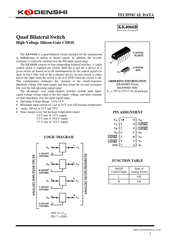
The KK4066B is a quad bilateral switch intended for the transmission or multiplexing of analog or digital signals. In addition, the on-state resistance is relatively constant over the full input-signal range. The KK4066B consists of four independent bilateral switches. A single control signal is required per switch. Both the p and the n device in a given switch are biased on or off simultaneously by the control signal.(As show in Fig.1.)The well of the n-channel device on each switch is either tied to the input when the switch is on or to GND when the switch is off. This configuration eliminates the variation of the switch-transistor threshold voltage with input signal, and thus keeps the on-state resistance low over the full operating-signal range. The advantages over single-channel switches include peak inputsignal voltage swings equal to the full supply voltage, and more constant on-state impedance over the input-signal range.
- Operating Voltage Range: 3.0 to 18 V
- Maximum input current of 1 µA at 18 V over full package-temperature
- range; 100 n A at 18 V and 25°C
- Noise margin (over full package temperature range): 1.0 V min @ 5.0 V supply 2.0 V min @ 10.0 V supply 2.5 V min @ 15.0 V supply
ORDERING INFORMATION KK4066BN Plastic KK4066BD SOIC TA = -55° to 125° C for all packages
PIN ASSIGNMENT
LOGIC DIAGRAM
FUNCTION TABLE
On/Off Control Input L H State of Analog Switch Off On
PIN 14 =VCC PIN 7 = GND
..
MAXIMUM RATINGS-
Symbol VCC VIN VOUT IIN PD PD Tstg TL
- Parameter DC Supply Voltage (Referenced to GND) DC Input Voltage (Referenced to GND) DC Output Voltage (Referenced to GND) DC Input Current, per Pin Power Dissipation in Still Air, Plastic DIP+ SOIC Package+ Power Dissipation per Output Transistor Storage Temperature Lead Temperature, 1 mm from Case for 10 Seconds (Plastic DIP or SOIC Package)
Value -0.5 to +20 -0.5 to...