KK4093B
KK4093B is Quad 2-Input NAND Schmitt Triggers High-Voltage Silicon-Gate CMOS manufactured by Kodenshi AUK Group.
..
TECHNICAL DATA
Quad 2-Input NAND Schmitt Triggers
High-Voltage Silicon-Gate CMOS
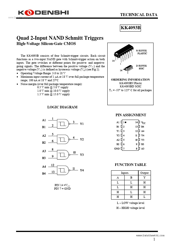
The KK4093B consists of four Schmitt-trigger circuits. Each circuit functions as a two-input NAND gate with Schmitt-trigger action on both inputs. The gate switches at different points for positive- and negativegoing signals. The difference between the positive voltage (VТ+) and the negative voltage (VТ-) is defined as hysteresis voltage (VH) (see Fig.1).
- Operating Voltage Range: 3.0 to 18 V
- Maximum input current of 1 µA at 18 V over full package-temperature range; 100 n A at 18 V and 25°C
- Noise margin (over full package temperature range): 0.5 V min @ 5.0 V supply 1.0 V min @ 10.0 V supply 1.5 V min @ 15.0 V supply
ORDERING INFORMATION KK4093BN Plastic KK4093BD SOIC TA = -55° to 125° C for all packages
LOGIC DIAGRAM PIN ASSIGNMENT
FUNCTION TABLE
Inputs A PIN 14 =VCC PIN 7 = GND L L H H B L H L H Output Y H H H L
- LOW voltage level H
- HIGH voltage level
..
MAXIMUM RATINGS-
Symbol VCC VIN IIN PD Ptot Tstg TL
- Parameter DC Supply Voltage (Referenced to GND) DC Input Voltage (Referenced to GND) DC Input Current, per Pin Power Dissipation in Still Air, Plastic DIP+ SOIC Package+ Power Dissipation per Output Transistor Storage Temperature Lead Temperature, 1 mm from Case for 10 Seconds (Plastic DIP or SOIC Package)
Value -0.5 to +20 -0.5 to VCC +0.5 ±10 500 500 100 -65 to +150 260
Unit V V m A m W m W °C °C
Maximum Ratings are those values beyond which damage to the device may occur. Functional operation should be restricted to the Remended Operating Conditions. +Derating
- Plastic DIP:
- 12 m W/°C from 100° to 125°C SOIC Package: :
- 7 m W/°C from 65° to 125°C
REMENDED OPERATING CONDITIONS
Symbol VCC VIN, VOUT TA Parameter DC Supply Voltage (Referenced to GND) DC Input Voltage, Output Voltage (Referenced to GND) Operating Temperature, All Package Types Min 3.0 0 -55 Max 18 VCC +125 Unit V V °C
This device...