KK74HC365A
KK74HC365A is Hex 3-State Noninverting Buffer manufactured by Kodenshi AUK Group.
TECHNICAL DATA
Hex 3-State Noninverting Buffer with mon Enables
High-Performance Silicon-Gate CMOS
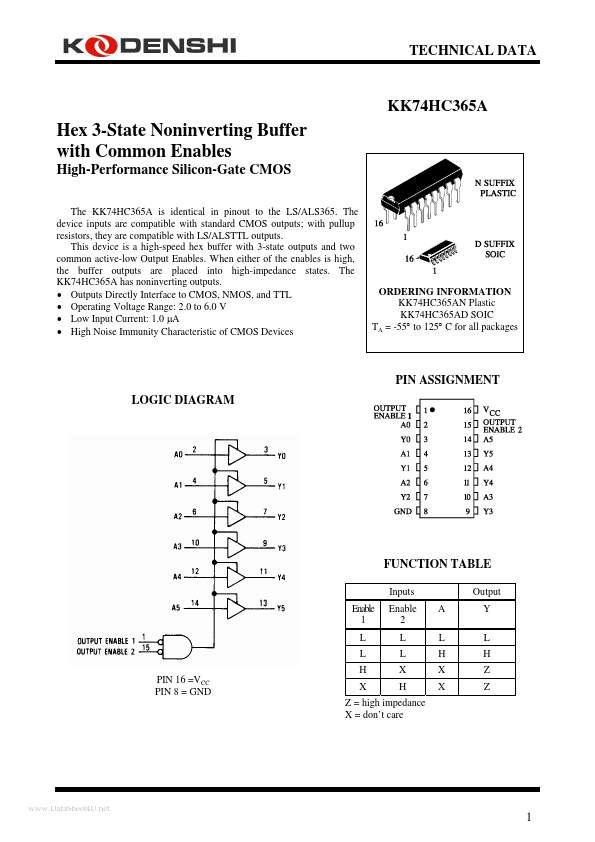
The KK74HC365A is identical in pinout to the LS/ALS365. The device inputs are patible with standard CMOS outputs; with pullup resistors, they are patible with LS/ALSTTL outputs. This device is a high-speed hex buffer with 3-state outputs and two mon active-low Output Enables. When either of the enables is high, the buffer outputs are placed into high-impedance states. The KK74HC365A has noninverting outputs.
- Outputs Directly Interface to CMOS, NMOS, and TTL
- Operating Voltage Range: 2.0 to 6.0 V
- Low Input Current: 1.0 µA
- High Noise Immunity Characteristic of CMOS Devices
ORDERING INFORMATION KK74HC365AN Plastic KK74HC365AD SOIC TA = -55° to 125° C for all packages
PIN ASSIGNMENT LOGIC DIAGRAM
FUNCTION TABLE
Inputs Enable 1 L L H PIN 16 =VCC PIN 8 = GND X Enable 2 L L X H A L H X X Output Y L H Z Z
Z = high impedance X = don’t care
..net
MAXIMUM RATINGS-
Symbol VCC VIN VOUT IIN IOUT ICC PD Tstg TL
- Parameter DC Supply Voltage (Referenced to GND) DC Input Voltage (Referenced to GND) DC Output Voltage (Referenced to GND) DC Input Current, per Pin DC Output Current, per Pin DC Supply Current, VCC and GND Pins Power Dissipation in Still Air, Plastic DIP+ SOIC Package+ Storage Temperature Lead Temperature, 1 mm from Case for 10 Seconds (Plastic DIP or SOIC Package)
Value -0.5 to +7.0 -1.5 to VCC +1.5 -0.5 to VCC +0.5 ±20 ±35 ±75 750 500 -65 to +150 260
Unit V V V m A m A m A m W °C °C
Maximum Ratings are those values beyond which damage to the device may occur. Functional operation should be restricted to the Remended Operating Conditions. +Derating
- Plastic DIP:
- 10 m W/°C from 65° to 125°C SOIC Package: :
- 7 m W/°C from 65° to 125°C
REMENDED OPERATING CONDITIONS
Symbol VCC VIN, VOUT TA tr, tf Parameter DC Supply Voltage (Referenced to GND) DC Input Voltage, Output Voltage (Referenced to GND)...