KK74HC373A
KK74HC373A is Octal 3-State Noninverting manufactured by Kodenshi AUK Group.
TECHNICAL DATA
Octal 3-State Noninverting Transparent Latch
High-Performance Silicon-Gate CMOS
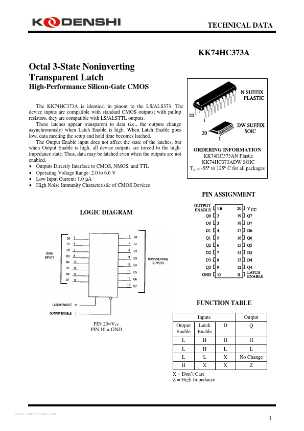
The KK74HC373A is identical in pinout to the LS/ALS373. The device inputs are patible with standard CMOS outputs; with pullup resistors, they are patible with LS/ALSTTL outputs. These latches appear transparent to data (i.e., the outputs change asynchronously) when Latch Enable is high. When Latch Enable goes low, data meeting the setup and hold time bees latched. The Output Enable input does not affect the state of the latches, but when Output Enable is high, all device outputs are forced to the highimpedance state. Thus, data may be latched even when the outputs are not enabled.
- Outputs Directly Interface to CMOS, NMOS, and TTL
- Operating Voltage Range: 2.0 to 6.0 V
- Low Input Current: 1.0 µA
- High Noise Immunity Characteristic of CMOS Devices
ORDERING INFORMATION KK74HC373AN Plastic KK74HC373ADW SOIC TA = -55° to 125° C for all packages
PIN ASSIGNMENT LOGIC DIAGRAM
FUNCTION TABLE
Inputs PIN 20=VCC PIN 10 = GND Output Enable L L L H Latch Enable H H L X D H L X X Output Q H L No Change Z
X = Don’t Care Z = High Impedance
..net
MAXIMUM RATINGS-
Symbol VCC VIN VOUT IIN IOUT ICC PD Tstg TL
- Parameter DC Supply Voltage (Referenced to GND) DC Input Voltage (Referenced to GND) DC Output Voltage (Referenced to GND) DC Input Current, per Pin DC Output Current, per Pin DC Supply Current, VCC and GND Pins Power Dissipation in Still Air, Plastic DIP+ SOIC Package+ Storage Temperature Lead Temperature, 1 mm from Case for 10 Seconds (Plastic DIP or SOIC Package)
Value -0.5 to +7.0 -1.5 to VCC +1.5 -0.5 to VCC +0.5 ±20 ±35 ±75 750 500 -65 to +150 260
Unit V V V m A m A m A m W °C °C
Maximum Ratings are those values beyond which damage to the device may occur. Functional operation should be restricted to the Remended Operating Conditions. +Derating
- Plastic DIP:
- 10 m W/°C from 65° to 125°C SOIC Package: :
- 7 m W/°C...