KK74HCT109A
KK74HCT109A is Dual J-K Flip-Flop manufactured by Kodenshi AUK Group.
TECHNICAL DATA
KK74HCT109A Dual J-K Flip-Flop with set and Reset High-Performance Silicon-Gate CMOS
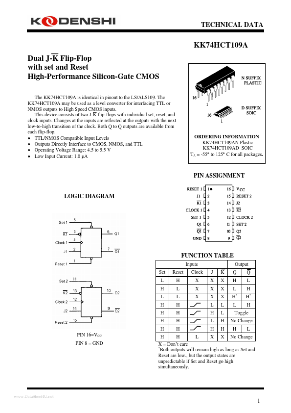
The KK74HCT109A is identical in pinout to the LS/ALS109. The KK74HCT109A may be used as a level converter for interfacing TTL or NMOS outputs to High Speed CMOS inputs. This device consists of two J-K flip-flops with individual set, reset, and clock inputs. Changes at the inputs are reflected at the outputs with the next low-to-high transition of the clock. Both Q to Q outputs are available from each flip-flop.
- TTL/NMOS patible Input Levels
- Outputs Directly Interface to CMOS, NMOS, and TTL
- Operating Voltage Range: 4.5 to 5.5 V
- Low Input Current: 1.0 µA
ORDERING INFORMATION KK74HCT109AN Plastic KK74HCT109AD SOIC TA = -55° to 125° C for all packages.
PIN ASSIGNMENT
LOGIC DIAGRAM
FUNCTION TABLE
Inputs Set L H L H H H H PIN 16=VCC PIN 8 = GND Reset H L L H H H H Clock X X X J X X X L H L H K X X X L L H H Output Q H L H
- Q L H H- H
Toggle No Change H L
H H L X X No Change X = Don’t care
- Both outputs will remain high as long as Set and Reset are low., but the output states are unpredictable if Set and Reset go high simultaneously.
..net
MAXIMUM RATINGS-
Symbol VCC VIN VOUT IIN IOUT ICC PD Tstg TL
- Parameter DC Supply Voltage (Referenced to GND) DC Input Voltage (Referenced to GND) DC Output Voltage (Referenced to GND) DC Input Current, per Pin DC Output Current, per Pin DC Supply Current, VCC and GND Pins Power Dissipation in Still Air, Plastic DIP+ SOIC Package+ Storage Temperature Lead Temperature, 1 mm from Case for 10 Seconds (Plastic DIP or SOIC Package)
Value -0.5 to +7.0 -1.5 to VCC +1.5 -0.5 to VCC +0.5 ±20 ±25 ±50 750 500 -65 to +150 260
Unit V V V m A m A m A m W °C °C
Maximum Ratings are those values beyond witch damage to the device may occur. Functional operation should be restricted to the Remended Operating Conditions. +Derating
- Plastic DIP:
- 10 m W/°C from 65° to 125°C SOIC Package: :
- 7 m...