KK4006B
KK4006B is CMOS 18-Stage Static Shift Register manufactured by Kodenshi AUK Group.
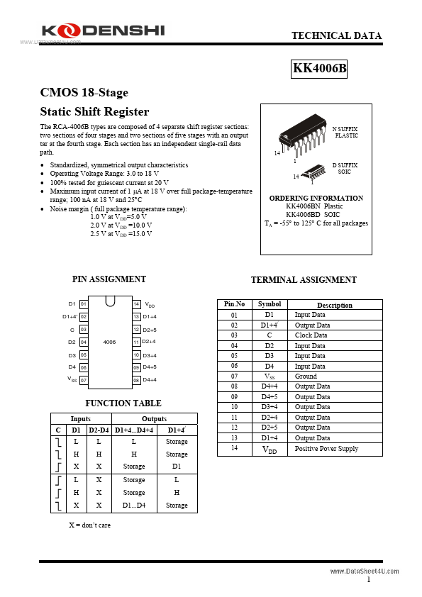
Description
Input Data Output Data Clock Data Input Data Input Data Input Data Ground Output Data Output Data Output Data Output Data Output Data Output Data
Positive Pover Supply
X = don’t care
..
MAXIMUM RATINGS-
Symbol VDD VIN IIN PD Ptot Tstg TL
- Parameter DC Supply Voltage (Referenced to GND) DC Input Voltage (Referenced to GND) DC Input Current, per Pin Power Dissipation in Still Air, Plastic DIP, SOIC Package Power Dissipation per Output Transistor Storage Temperature Lead Temperature, 1 mm from Case for 10 Seconds (Plastic DIP or SOIC Package)
Value -0.5 to +20 -0.5 to VDD +0.5 ±10 500-
- 100 -65 to +150 260
Unit V V m A m W m W °C °C
Maximum Ratings are those values beyond which damage to the device may occur. Functional operation should be restricted to the Remended Operating Conditions.
- - Derating:
- Plastic DIP from -55 to +100°C
- SOIC Package from -55 to +65°C
- Plastic DIP:
- 12 m W/°C from +100 to +125°C
- SOIC Package: :
- 7 m W/°C from +65 to +125°C
REMENDED OPERATING CONDITIONS
Symbol VCC VIN TA Parameter DC Supply Voltage (Referenced to GND) DC Input Voltage (Referenced to GND) Operating Temperature, All Package Types Min 3.0 0 -55 Max 18 VCC +125 Unit V V °C
This device contains protection circuitry to guard against damage due to high static voltages or electric fields. However, precautions must be taken to avoid applications of any voltage higher than maximum rated voltages to this high-impedance circuit. For proper operation VIN should be constrained to the range GND≤VIN ≤VCC. Unused inputs must always be tied to an appropriate logic voltage level (e.g., either Vss or VDD). Unused outputs must be left open.
..
DC ELECTRICAL CHARACTERISTICS
Symbol Parameter Test...