KK472
KK472 is Liquid Crystal Display Controller manufactured by Kodenshi AUK Group.
Description
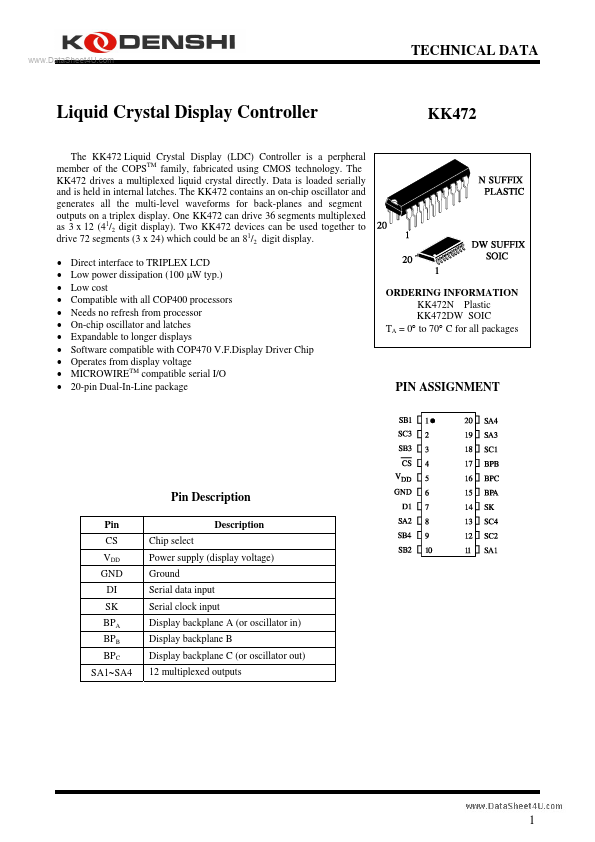
Pin CS VDD GND DI SK BPA BPB BPC SA1∼SA4 Chip select Power supply (display voltage) Ground Serial data input Serial clock input Display backplane A (or oscillator in) Display backplane B Display backplane C (or oscillator out) 12 multiplexed outputs Description
..
DC ELECTRICAL CHARACTERISTICS (GND=0 V, VDD=3.0 V to 5.5 V, TA= 0°C to 70°C (depends on display characteristics) Guaranteed Limit Symbol VDD IDD VIL VIH VIL VIH VOL VOH VBPA,BPB,BPC ON VBPA,BPB,BPC OFF VBPA,BPB,BPC ON VBPA,BPB,BPC OFF VSEG ON VSEG OFF VSEG ON VSEG OFF Internal Oscillator Frequency Frame Time (Int. Osc. ÷ 192) 1/TSCAN Scan Frequency SK Clock Frequency SK Width t SETUP t HOLD t SETUP t HOLD Output Loading Capacitance Note 2: ∆V
- 0.05VDD. DI Data Stup DI Data Hold CS Segment Outputs (SA1 ∼ SA4) Segment Outputs (SA1 ∼ SA4) Backplane Outputs (BPA,BPB,BPC) During BP
- Time During BP + Time During BP
- Time 0 2/3VDD -∆V 0 2/3VDD -∆V VDD -∆V 1/3VDD -∆V 15 2.4 39 4 1.7 1.0 100 1.0 1.0 100 p F ∆V 2/3VDD +∆V ∆V 2/3VDD +∆V VDD 1/3VDD +∆V 80 12.8 208 250 k Hz ms Hz k Hz µs µs ns µs V V Backplane Outputs (BPA,BPB,BPC) During BP + Time VDD -∆V 1/3VDD -∆V VDD 1/3VDD +∆V V Output Levels, BPC (as Osc. Out) VDD-0.4 BPA (as Osc. in) VDD-0.6 Parameter Power Supply Voltage Power Supply Current (Note 1) Input Levels DI, SK, CS 0.7 VDD VDD =5.5 V Test Conditions Min 3.0 Max 5.5 250 0.8 VDD 0.6 VDD 0.4 VDD V V V Uni t V µA V
Note 1: Power supply current as measured in stand-alone mode with all outputs open and all inputs at VDD.
..
Figure 1. Serial Load Timing Diagram
Figure 2. Backplane and Segment Waveforms
..
N SUFFIX PLASTIC DIP (MS
- 001AD)
Dimension, mm
20 11 B 1 10
Symbol A B C
MIN 24.89 6.1
MAX 26.92 7.11 5.33
0.36 1.14 2.54 7.62 0° 2.92 7.62 0.2 0.38
0.56 1.78
C...