KK82C55
KK82C55 is CHMOS PROGRAMMABLE PERIPHERAL INTERFACE manufactured by Kodenshi AUK Group.
FEATURES
- -
- -
- -
- -
- - patible with all Intel and Most Other Microprocessors High Speed, «Zero Wait State» Operation with 8MHz 8086/88 and 80186/188 24 Programmable I/O Pins Low Power CHMOS pletely TTL patible Control Word Read-Back Capability Direct Bit Set/Reset Capability 2.5m A DC Drive Capability on all I/O Port Outputs Available in 40-Pin DIP Available in EXPRESS
- Standard Temperature Range
- Extended Temperature Range http://..net/
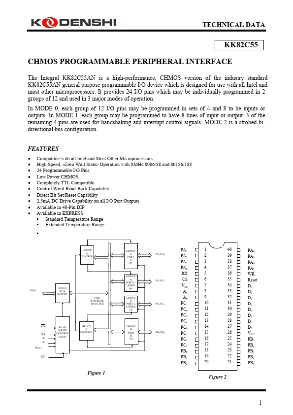
- PA3 PA2 PA1 PA0 RD CS VSS A1 A0 PC7 PC6 PC5 PC4 PC0 PC1 PC2 PC3 PB0 PB1 PB2 1. 2. 3. 4. 5. 6. 7. 8. 9. 10 11 12 13 14 15 16 17 18 19 20 40 39 38 37 36 35 34 33 32 31 30 29 28 27 26 25 24 23 22 21 PA4 PA5 PA6 PA7 WR Reset D0 D1 D2 D3 D4 D5 D6 D7 VCC PB7 PB6 PB5 PB4 PB3
GROUP A CONTROL
GROUP A PORT A (8)
PA7-PA0
D7-D0
DATA BUS BUFFER 8 BIT INTERNAL DATA BUS
GROUP A PORT C UPPER (4) GROUP B PORT C LOWER (4)
PC7-PC4
PC3-PC0
RD WR A1 A0 Reset
READ/ WRITE CONTROL LOGIC
GROUP B CONTROL
GROUP B PORT B (8)
PB7-PB0
Figure 1
Figure 2
1 datasheet pdf
- http://..net/
KK82C55A
Symbol PA3-0
RD CS
Pin number 1-4 5 6 7 8-9
Type I/O I I
Name and Function PORT A, PINS 0-3: Lower nibble of an 8-bit data output latch buffer and an 8-bit data input latch. READ CONTROL: This input is low during CPU read operations. CHIP SELECT: A low on this input enables the 82C55A to respond to RD and WR signals RD and WR are ignored otherwise. System Ground. ADDRESS: These input signals in conjunction RD and WR control the selection of one of the three ports or the control word registers. Input Operation (Read) A1 A0 CS WR RD Port A
- Data Bus 0 0 0 1 0 Port B
- Data Bus 0 1 0 1 0 Port C
- Data Bus 1 0 0 1 0 Control Word
- Data Bus 1 1 0 1 0
Output Operation (Write)
GND...