KKA3654
KKA3654 is VERTICAL DEFLECTION AND GUARD CIRCUIT manufactured by Kodenshi AUK Group.
FEATURES
- -
- - Direct drive to the deflection coils 90 and 110 deflection system Internal blanking guard circuit Internal voltage stabilizer
QUICK REFERENCE DATA
PARAMETER Output voltage Output current (peak-to-peak) Supply voltage Guard circuit output voltage Operating ambient temperature range Storage temperature THERMAL RESISTANCE From junction to mounting base SYMBOL V5-2 I5(p-p) V9-2 V7-2 Tamb Tstg
Rth j-mb
MIN.
- 25
- 55
3,5
MAX. 60 3 40 5,6 60 150
UNIT V A V V o C o C
K/W
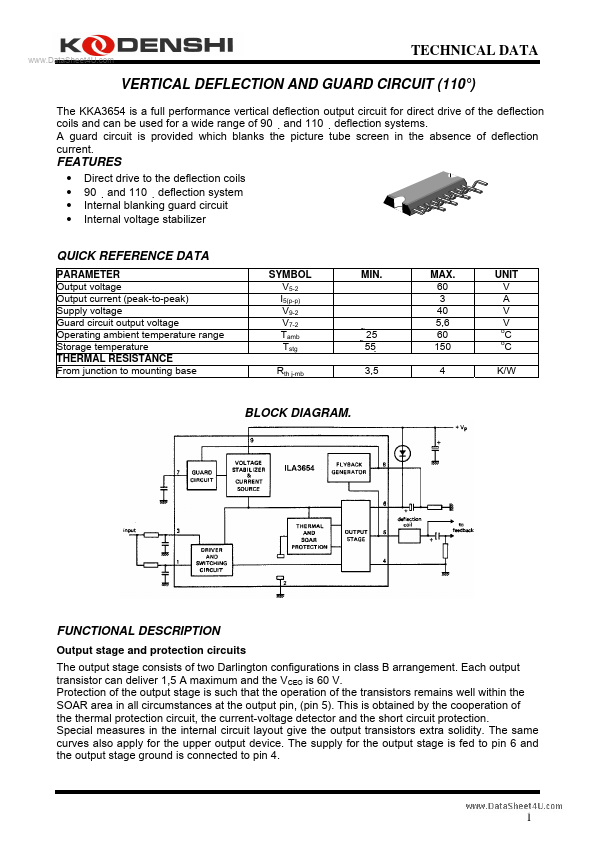
BLOCK DIAGRAM.
FUNCTIONAL DESCRIPTION
Output stage and protection circuits The output stage consists of two Darlington configurations in class B arrangement. Each output transistor can deliver 1,5 A maximum and the VCEO is 60 V. Protection of the output stage is such that the operation of the transistors remains well within the SOAR area in all circumstances at the output pin, (pin 5). This is obtained by the cooperation of the thermal protection circuit, the current-voltage detector and the short circuit protection. Special measures in the internal circuit layout give the output transistors extra solidity. The same curves also apply for the upper output device. The supply for the output stage is fed to pin 6 and the output stage ground is connected to pin 4.
..
Driver and switching circuit Pin 1 is the input for the driver of the output stage. The signal at pin 1 is also applied to pin 3 which is the input of a switching circuit (pin 1 and 3 are connected via external resistors). This switching circuit rapidly turns off the lower output stage when the flyback starts and it, therefore, allows a quick start of the flyback generator. The maximum required input signal for the maximum output current peak-to-peak value of 3 A is only 3 V, the sum of the currents in pins 1 and 3 is then maximum 1 m A. Flyback generator During scan, the capacitor between pins 6 and 8 is charged to a level which is dependent on the value of the resistor at pin 8 (see Block diagram )....