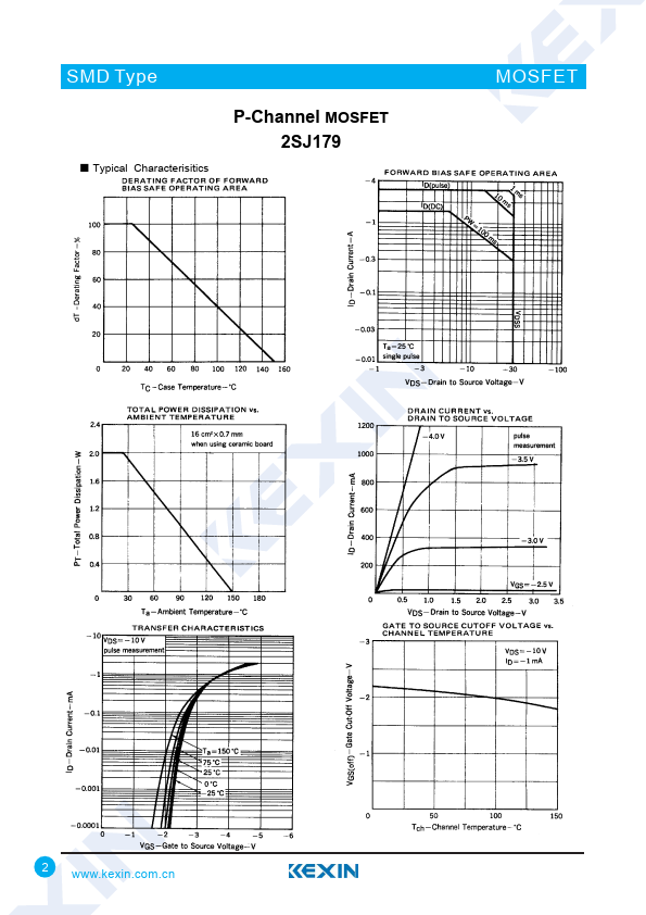
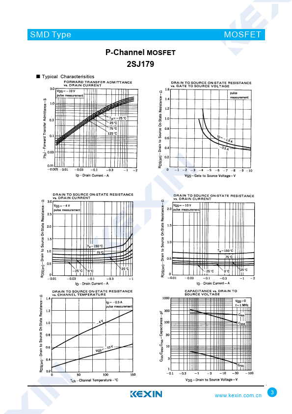
Kexin Electronics 2SJ179
P-Channel MOSFET
| Part No. | 2SJ179 |
|---|---|
| Datasheet | 2SJ179 Download |
| Manufacturer | Kexin Electronics |
| Description | P-Channel MOSFET |
| Buy | Stock & Price |
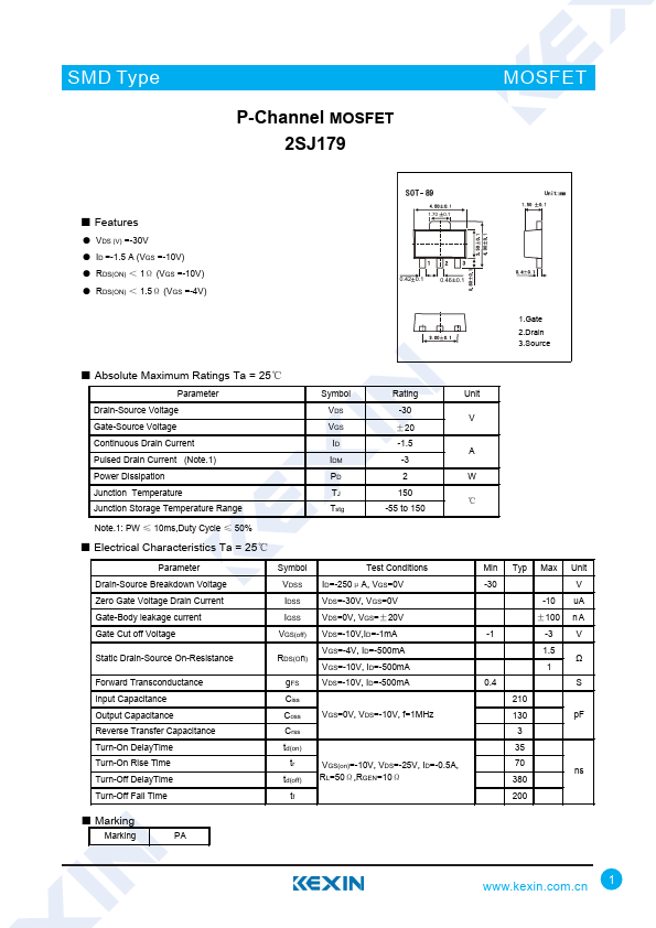
FEATURES
● VDS (V) =-30V● ID =-1.5 A (VGS =-10V)
● RDS(ON) < 1Ω (VGS =-10V)
● RDS(ON) < 1.5Ω (VGS =-4V) 1.70 0.1 0.42 0.1 0.46 0.1 1.Gate 2.Drain 3.Source
●
ABSOLUTE MAXIMUM RATINGS
Ta = 25℃ Parameter Drain-Source Voltage Gate-Source Voltage Continuous Drain Current Pulsed Drain Current (Note.1) Power Dissipation Junction Temperature Junction Storage Temperature Range Symbol Rating Unit VDS -30 V VGS ±20 ID -1.5 A IDM -3 PD 2 W TJ 150 ℃ Tstg -55 to 150 Note.1: PW ≤ 10ms,Duty Cycle ≤ 50%●
ELECTRICAL CHARACTERISTICS
Ta = 25℃ Parameter Drain-Source Breakdown Voltage Zero Gate Voltage Drain Current Gate-Body leakage current Gate Cut off Voltage Static Drain-Source On-Resistance Forward Transconductance Input Capacitance Output Capacitance Reverse Transfer Capacitance Turn-On DelayTime Turn-On Rise Time Turn-Off DelayTime Turn-Off Fall Time Symbol Test Conditions Min VDSS ID=-250μA, VGS=0V -30 IDSS VDS=-30V, VGS=0V IGSS VDS=0V, VGS=±20V VGS(off) VDS=-10V,ID=-1mA -1 RDS(On) VGS=-4V, ID=-50...