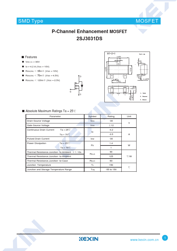
ƽ VDS (V) =-30V ƽ ID =-4.2 A (VGS =-10V) ƽ RDS(ON) ˘ 5m¡ (VGS =-10V) ƽ RDS(ON) ˘ m¡ (VGS =-4.5V) ƽ RDS(ON) ˘ 120m¡ (VGS =-2.5V)
D
G S
627
3
1
2
1.6
8QLW PP
.
DWH 6RXUFH 'UDLQ
Ƶ Absolute Maximum Ratings Ta = 25ć
Parameter Drain-Source Voltage
Gate-Source Voltage
Continuous Drain Current
Ta = 25ć
Ta = 70ć
Pulsed Drain.
The following content is an automatically extracted verbatim text
from the original manufacturer datasheet and is provided for reference purposes only.
View original datasheet text
SMD Type
P-Channel Enhancement MOSFET 6-'6
MOSFET
Ƶ Features
ƽ VDS (V) =-30V ƽ ID =-4.2 A (VGS =-10V) ƽ RDS(ON) ˘ 5m¡ (VGS =-10V) ƽ RDS(ON) ˘ m¡ (VGS =-4.5V) ƽ RDS(ON) ˘ 120m¡ (VGS =-2.5V)
D
G S
627
3
1
2
1.6
8QLW PP
*DWH 6RXUFH 'UDLQ
Ƶ Absolute Maximum Ratings Ta = 25ć
Parameter Drain-Source Voltage
Gate-Source Voltage
Continuous Drain Current
Ta = 25ć
Ta = 70ć
Pulsed Drain Current
Power Dissipation
Ta = 25ć
Ta = 70ć
Thermal Resistance.Junction- to-Ambient t İ 10s
Thermal Resistance.Junction- to-Ambient
Thermal Resistance.