Datasheet4U Logo Datasheet4U.com

2SJ602 - MOS Field Effect Transistor

Key Features

  • Low on-resistance RDS(on)1 = 73 m RDS(on)2 = 107m MAX. (VGS =-10 V, ID = -10 A) Low Ciss: Ciss = 1300 pF TYP. Built-in gate protection diode +0.2 5.28-0.2 +0.1 1.27-0.1 0.1max +0.1 0.81-0.1 2.54 5.08 +0.1 -0.1 +0.2 2.54-0.2 +0.2 15.25-0.2 MAX. (VGS = -4.0 V, ID =-10 A) +0.2 8.7-0.2 +0.2 2.54-0.2 +0.2 0.4-0.2 Absolute Maximum Ratings Ta = 25 Parameter Drain to source voltage Gate to source voltage Drain current (DC) Drain current(pulse).
  • Power dissipation TC=25 TA=25 Channel tempe.

📥 Download Datasheet

Full PDF Text Transcription (Reference)

The following content is an automatically extracted verbatim text from the original manufacturer datasheet and is provided for reference purposes only.

View original datasheet text
SMD Type MOS Field Effect Transistor 2SJ602
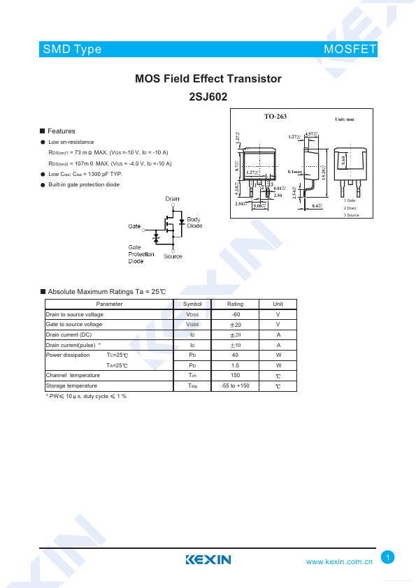
 TO-263 +0.1 1.27-0.1 MOSFET Unit: mm +0.1 1.27-0.1 +0.2 4.57-0.2 Features Low on-resistance RDS(on)1 = 73 m RDS(on)2 = 107m MAX. (VGS =-10 V, ID = -10 A) Low Ciss: Ciss = 1300 pF TYP. Built-in gate protection diode +0.2 5.28-0.2 +0.1 1.27-0.1 0.1max +0.1 0.81-0.1 2.54 5.08 +0.1 -0.1 +0.2 2.54-0.2 +0.2 15.25-0.2 MAX. (VGS = -4.0 V, ID =-10 A) +0.2 8.7-0.2 +0.2 2.54-0.2 +0.2 0.4-0.2 Absolute Maximum Ratings Ta = 25 Parameter Drain to source voltage Gate to source voltage Drain current (DC) Drain current(pulse) * Power dissipation TC=25 TA=25 Channel temperature Storage temperature * PW 10 s, duty cycle 1% Symbol VDSS VGSS ID ID PD PD Tch Tstg Rating -60 20 20 50 40 1.5 150 -55 to +150 Unit V V A A W W 5.