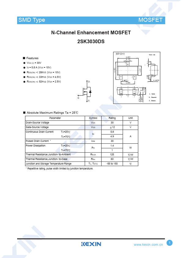
Datasheet4U Logo Datasheet4U.com

2SK3030DS - N-Channel Enhancement MOSFET

Key Features

  • VDS (V) = 30V ID = 5.8 A (VGS = 10V) RDS(ON) 28m (VGS = 10V) RDS(ON) 33m (VGS = 4.5V) RDS(ON) 52m (VGS = 2.5V) SOT-23-3 2.9 +0.2 -0.1 0.4 +0.1 -0.1 3 0.4 Unit: mm +0.2 1.6 -0.1 +0.2 2.8 -0.1 0.55 1 2 D 0.95 +0.1 -0.1 1.9 +0.1 -0.2 0.15 +0.02 -0.02 +0.2 1.1 -0.1 G S 0-0.1 +0.1 0.68 -0.1 1. Gate 2. Source 3. Drain Absolute Maximum Ratings Ta = 25 Parameter Drain-Source Voltage Gate-Source Voltage Continuous Drain Current TA=25 TA=70 Pulsed Drain Current.
  • Power Dissipat.

📥 Download Datasheet

Full PDF Text Transcription (Reference)

The following content is an automatically extracted verbatim text from the original manufacturer datasheet and is provided for reference purposes only.

View original datasheet text
SMD Type TraMnOsiSsFtoErsT N-Channel Enhancement MOSFET 2SK3030DS Features VDS (V) = 30V ID = 5.8 A (VGS = 10V) RDS(ON) 28m (VGS = 10V) RDS(ON) 33m (VGS = 4.5V) RDS(ON) 52m (VGS = 2.5V) SOT-23-3 2.9 +0.2 -0.1 0.4 +0.1 -0.1 3 0.4 Unit: mm +0.2 1.6 -0.1 +0.2 2.8 -0.1 0.55 1 2 D 0.95 +0.1 -0.1 1.9 +0.1 -0.2 0.15 +0.02 -0.02 +0.2 1.1 -0.1 G S 0-0.1 +0.1 0.68 -0.1 1. Gate 2. Source 3. Drain Absolute Maximum Ratings Ta = 25 Parameter Drain-Source Voltage Gate-Source Voltage Continuous Drain Current TA=25 TA=70 Pulsed Drain Current * Power Dissipation TA=25 TA=70 Thermal Resistance.Junction- to-Ambient Thermal Resistance.Junction- to-Case Junction and Storage Temperature Range Symbol VDS VGS ID IDM PD RthJA Rthc TJ, TSTG Rating 30 12 5.8 4.9 30 1.