2SK3639
2SK3639 is MOS Field Effect Transistor manufactured by Kexin Semiconductor.
Features
Low on-state resistance RDS(on)1 = 5.5 m MAX. (VGS = 10 V, ID = 32 A) RDS(on)2 = 8.5 m MAX. (VGS = 4.5 V, ID = 32 A) Low Ciss: Ciss = 2400 p F TYP.
+0.2 9.70 -0.2
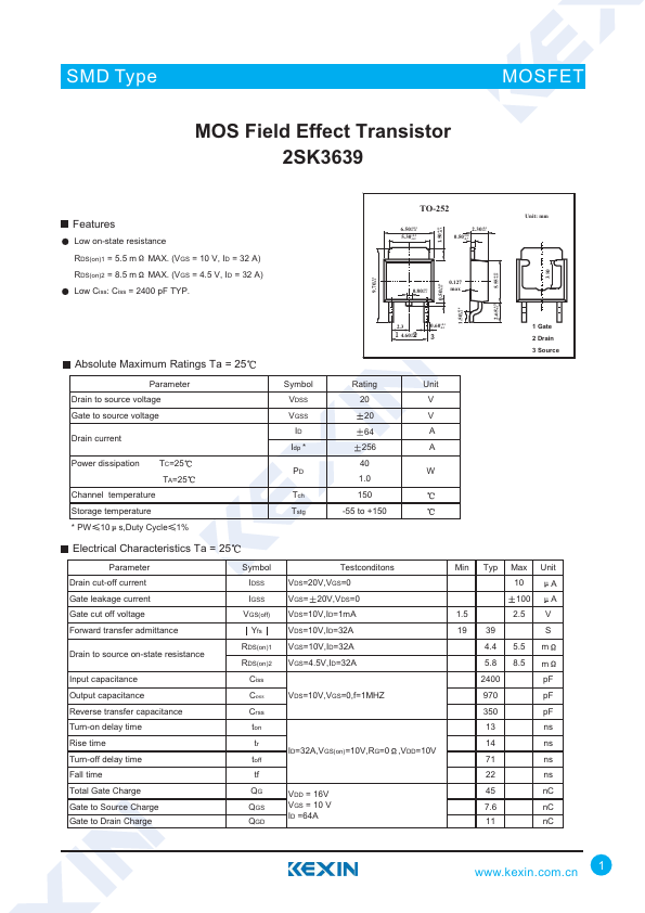
TO-252
6.50+0.15 -0.15
5.30+0.2 -0.2
2.30+0.1 -0.1
0.50+0.8 -0.7
Unit: mm
+0.15 1.50 -0.15
+0.15 5.55 -0.15
0.80+0.1 -0.1
0.127 max
+0.25 2.65 -0.1
+0.15 0.50 -0.15
+0.28 1.50 -0.1
Absolute Maximum Ratings Ta = 25
Parameter Drain to source voltage Gate to source voltage
Drain current
Power dissipation TC=25 TA=25
Channel temperature Storage temperature
- PW 10 s,Duty Cycle 1%
2.3 4.60+0.15
-0.15
0.60+0.1 -0.1
Symbol
Rating
Unit
VDSS
VGSS
Idp
-...