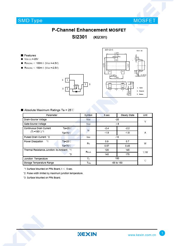
A1SHB
Key Features
- VDS (V) =-20V
- RDS(ON) < 100mΩ (VGS =-4.5V)
- RDS(ON) < 150mΩ (VGS =-2.5V) G1 S2 3D +0.22.8 -0.1 SOT-23-3
- 9 +0.2 -0.1
- 4 +0.1 -0.1 3 12 0.95 +0.1 -0.1
- 9 +0.1 -0.2 +0.21.1 -0.1 +0.21.6 -0.1
- 55 0.4 Unit: mm
- 15 +0.02 -0.02
- Source
- Drain 0-0.1 +0.10.68 -0.1
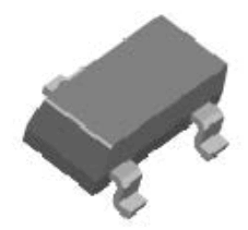
Representative A1SHB image (package may vary by manufacturer)