A9451
A9451 is P-Channel MOSFET manufactured by Kexin Semiconductor.
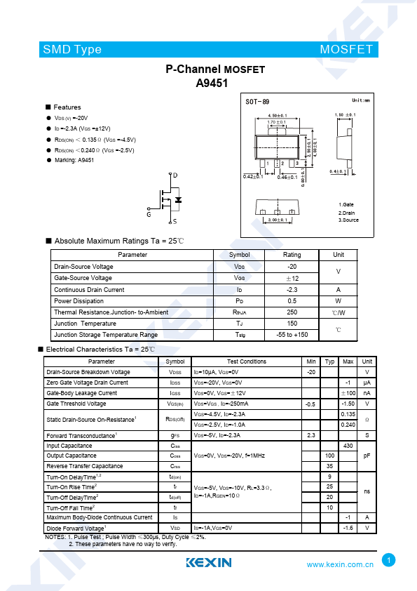
Features
- VDS (V) =-20V
- ID =-2.3A (VGS =±12V)
- RDS(ON) < 0.135Ω (VGS =-4.5V)
- RDS(ON) <0.240Ω (VGS =-2.5V)
- Marking: A9451
P-Channel MOSFET A9451
1.70 0.1
MOSFET
0.42 0.1
0.46 0.1
1.Gate 2.Drain 3.Source
- Absolute Maximum Ratings Ta = 25℃
Parameter Drain-Source Voltage Gate-Source Voltage Continuous Drain Current Power Dissipation Thermal Resistance.Junction- to-Ambient Junction Temperature Junction Storage Temperature Range
Symbol VDS VGS ID PD Rth JA TJ Tstg
Rating -20 ±12 -2.3 0.5 250 150
-55 to +150
Unit V
A W ℃/W ℃
- Electrical Characteristics Ta = 25℃
Parameter
Symbol
Test Conditions
Drain-Source Breakdown Voltage
VDSS ID=10μA, VGS=0V
Zero Gate Voltage Drain Current
IDSS
VDS=-20V, VGS=0V
Gate-Body Leakage Current
IGSS
VDS=0V, VGS=±12V
Gate Threshold Voltage
VGS(th) VDS=VGS , ID=-250m A
Static Drain-Source On-Resistance1
RDS(On)
VGS=-4.5V, ID=-2.3A VGS=-2.5V, ID=-1.0A
Forward Transconductance1 g FS
VDS=-5V, ID=-2.3A
Input Capacitance
Ciss...