FEATURES
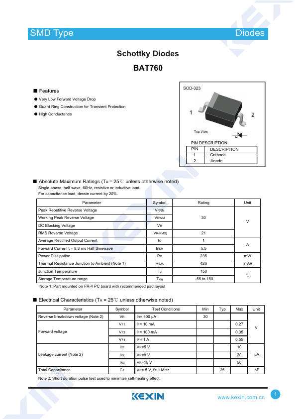
ƽ Very Low Forward Voltage Drop ƽ Guard Ring Construction for Transient Protection ƽ High Conductance SOD-323 1 2 Top View PIN DESCRIPTION
PIN DESCRIPTION
1 Cathode 2 Anode Ƶ ABSOLUTE MAXIMUM RATINGS
(TA = 25ć unless otherwise noted) Single phase, half wave, 60Hz, resistive or inductive load. For capacitance load, derate current by 20%. Parameter Symbol Peak Repetitive Reverse Voltage VRRM Working Peak Reverse Voltage VRWM DC Blocking Voltage VR RMS Reverse Voltage VR(RMS) Average Rectified Output Current IO Forward Current t = 8.3 ms Half Sinewave IFSM Power Dissipation PD Thermal Resistance Junction to Ambient (Note 1) RșJA Junction Temperature TJ Storage Temperature range Tstg Note 1: Part mounted on FR-4 PC board with recommended pad layout Ƶ ELECTRICAL CHARACTERISTICS
(TA = 25ć unless otherwise noted) Parameter Reverse breakdown voltage (Note 2) Forward voltage Leakage current (Note 2) Total Capacitance Symbol VR VF1 VF2 VF3 IR1 IR2 IR3 CT Test Conditions IR= 500 ȝA IF= 10 mA IF= 100 mA IF= 1 A VR=5 V VR=8 V VR=15 V VR= 5 V, f= 1 MHz Note 2: Short duration pulse test used to minimize self-heating effect.