F501
F501 is Silicon N-Channel Power MOSFET manufactured by Kexin Semiconductor.
Features
- VDS (V) = 500V
- ID = 0.03 A (VGS = 10V)
- RDS(ON) < 850 Ω (VGS = 10V)
- RDS(ON) < 750 Ω (VGS = 0V)
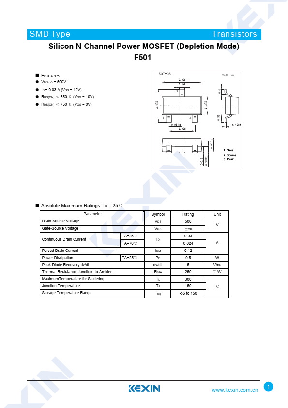
+0.1 2.4 -0.1
SOT-23
2.9 +0.1 -0.1
0.4 +0.1 -0.1
0.95 +0.1 -0.1 1.9 +0.1 -0.1
+0.1 1.3 -0.1
Unit: mm 0.1 +0.05
-0.01
+0.1 0.97 -0.1
1. Gate 2. Source 3. Drain
0-0.1 +0.1 0.38
-0.1
- Absolute Maximum Ratings Ta = 25℃
Parameter
Drain-Source Voltage
Gate-Source Voltage
Continuous Drain Current Pulsed Drain Current
TA=25℃ TA=70℃
Power Dissipation Peak Diode Recovery dv/dt
TA=25℃
Thermal Resistance.Junction- to-Ambient
Maximum Temperature for Soldering
Junction Temperature Storage Temperature Range
Symbol VDS VGS
IDM PD dv/dt RθJA TL TJ Tstg
Rating 500 ±20 0.03 0.024 0.12 0.5 5 250 300 150
-55 to 150
Unit...