FDB4020P
FDB4020P is P-Channel MOSFET manufactured by Kexin Semiconductor.
SMD Type
MOSFET
P-Channel 2.5V Specified Enhancement Mode Field Effect Transistor
KDB4020P(FDB4020P)
Features
-16 A, -20 V. RDS(on) = 0.08 Ù @ VGS = -4.5 V RDS(on) = 0.11 Ù @ VGS = -2.5 V.
Critical DC electrical parameters specified at elevated temperature. High density cell design for extremely low RDS(on).
+0.25.28 -0.2
+0.28.7 -0.2
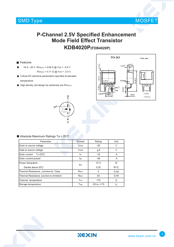
TO-263
+0.2
4.57+0.1 -0.2 1.27-0.1
Unit: mm
+0.11.27 -0.1
+0.22.54 -0.2 15.25-+00..22 5.60
1.27+0.1 -0.1
0.1max
2.54+0.2 -0.2
5.08+0.1 -0.1
0.81+0.1 -0.1
0.4+0.2 -0.2
1 Gate 2 Drain 3...