FDC2512
FDC2512 is N-Channel Enhancement MOSFET manufactured by Kexin Semiconductor.
Features
ƽ VDS (V) = 150V ƽ ID = 1.4A (VGS = 10V) ƽ RDS(ON) ˘ 425m¡ (VGS = 10V) ƽ RDS(ON) ˘ 475m¡ (VGS = 6V)
D D G
D D S
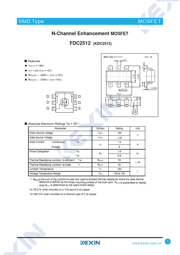
( SOT-23-6 ) 0.4+0.1
-0.1
+0.01 -0.01
+0.2 -0.1
1.6
2.8
8QLW PP
Ƶ Absolute Maximum Ratings Ta = 25ć
Parameter
Drain-Source Voltage
Gate-Source Voltage
Drain Current
- Continuous
- 1a
- Pulsed
Power Dissipation
- 1a
- 1b
Thermal Resistance.Junction- to-Ambient
- 1a
Thermal Resistance.Junction- to-Case
- 1
Junction Temperature
Storage Temperature...