NTR1P02LT1 Overview
Key Specifications
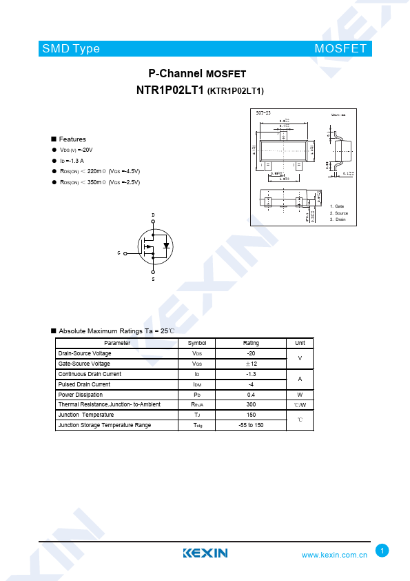
Package: SOT-23-3
Pins: 3
Height: 940 µm
Length: 2.9 mm
Key Features
- VDS (V) =-20V
- RDS(ON) < 220mΩ (VGS =-4.5V)
- 0.01 +0.1 0.97 -0.1
- Gate 0-0.1 +0.1 0.38
| Part | NTR1P02LT1 |
|---|---|
| Description | P-Channel MOSFET |
| Category | MOSFET |
| Manufacturer | Kexin Semiconductor |
| Size | 1.34 MB |
Package: SOT-23-3
Pins: 3
Height: 940 µm
Length: 2.9 mm
| Seller | Inventory | Price Breaks | Buy |
|---|---|---|---|
| Future Electronics | 468000 | 3000+ : 0.107 USD 9000+ : 0.105 USD 15000+ : 0.103 USD 30000+ : 0.102 USD |
View Offer |
| Future Electronics | 96000 | 3000+ : 0.107 USD 9000+ : 0.105 USD 15000+ : 0.103 USD 30000+ : 0.102 USD |
View Offer |
| Part Number | Manufacturer | Description |
|---|---|---|
| NTR1P02L | onsemi | P-Channel Power MOSFET |
| NTR1P02T1 | onsemi | Power MOSFET |
| NTR1P02 | onsemi | Power MOSFET |
| NTR1P02T3G | onsemi | Power MOSFET |
| NTR1P02T1G | onsemi | Power MOSFET |