NTR4501NT1G Overview
Key Features
- VDS (V) = 20V
- ID = 3.2 A (VGS = 4.5V)
- RDS(ON) < 70mΩ (VGS = 4.5V)
- RDS(ON) < 85mΩ (VGS = 2.5V)
- Leading Planar Technology for Low Gate Charge / Fast Switching
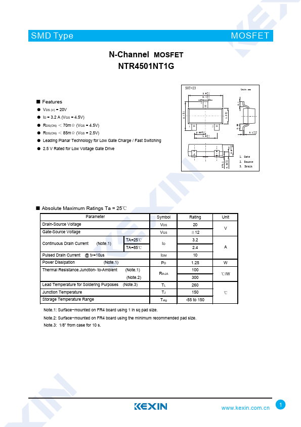
- Drain 0-0.1 +0.10.38
| Part | NTR4501NT1G |
|---|---|
| Description | N-Channel MOSFET |
| Category | MOSFET |
| Manufacturer | Kexin Semiconductor |
| Size | 1.37 MB |
| Part Number | Manufacturer | Description |
|---|---|---|
| NTR4501NT1G | VBsemi | N-Channel MOSFET |
| NTR4501NT1G | CANYU | N-Channel MOSFET |
| NTR4501N | onsemi | N-Channel Power MOSFET |