RDS(ON) < 20mΩ (VGS =-4.5V)
S G
D
1212-8 (DFN)
3.30 mm
D
8
D
7
D
6 D
5
S
1
S
3.30 mm
2
S
3
G
4
Bottom View.
Absolute Maximum Ratings Ta = 25℃
Drain-Source Voltage Gate-Source Voltage
Parameter
Continuous Drain Current
Pulsed Drain Current Avalanche Current Single-Pulse Avalanche Energy
Power Dissipation
Thermal Resistance. Junction- to-Ambient Thermal Resistance. Junction- to-.
The following content is an automatically extracted verbatim text
from the original manufacturer datasheet and is provided for reference purposes only.
View original datasheet text
SMD Type
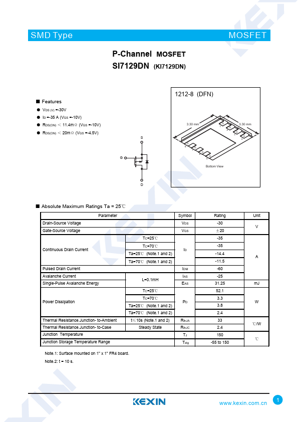
P-Channel MOSFET SI7129DN (KI7129DN)
MOSFET
■ Features
● VDS (V) =-30V ● ID =-35 A (VGS =-10V) ● RDS(ON) < 11.4mΩ (VGS =-10V) ● RDS(ON) < 20mΩ (VGS =-4.5V)
S G
D
1212-8 (DFN)
3.30 mm
D
8
D
7
D
6 D
5
S
1
S
3.30 mm
2
S
3
G
4
Bottom View
■ Absolute Maximum Ratings Ta = 25℃
Drain-Source Voltage Gate-Source Voltage
Parameter
Continuous Drain Current
Pulsed Drain Current Avalanche Current Single-Pulse Avalanche Energy
Power Dissipation
Thermal Resistance.Junction- to-Ambient Thermal Resistance.Junction- to-Case Junction Temperature Junction Storage Temperature Range
TC=25℃ TC=70℃ Ta=25℃ (Note.1 and 2) Ta=70℃ (Note.1 and 2)
L=0.1mH
TC=25℃ TC=70℃ Ta=25℃ (Note.1 and 2) Ta=70℃ (Note.1 and 2) t≤10s (Note.