SI9435BDY
SI9435BDY is P-Channel Enhancement MOSFET manufactured by Kexin Semiconductor.
Features
- VDSS = -30V
- ID = -5.7A (VGS = -10V)
- RDS(ON) = 42 mΩ @ VGS = -10 V
- RDS(ON) = 70 mΩ @ VGS = -4.5 V
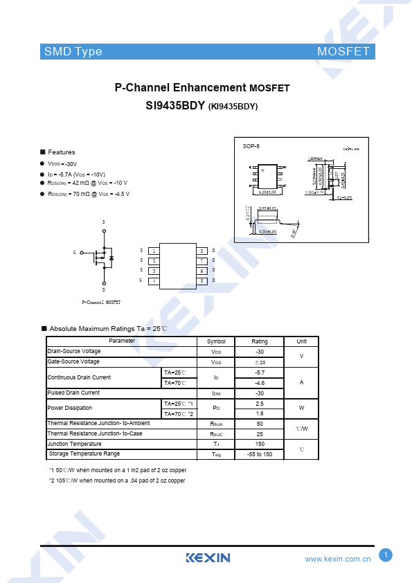
SOP-8
1.50 0.15
+0.04 0.21 -0.02
D P-Channel MOSFET
S1 S2 S3 G4
8D 7D 6D 5D
- Absolute Maximum Ratings Ta = 25℃
Parameter
Drain-Source Voltage
Gate-Source Voltage
Continuous Drain Current Pulsed Drain Current
TA=25℃ TA=70℃
Power Dissipation
Thermal Resistance.Junction- to-Ambient Thermal Resistance.Junction- to-Case Junction Temperature Storage Temperature Range
TA=25℃
- 1 TA=70℃
- 2
- 1 50℃/W when mounted on a 1 in2 pad of 2 oz copper
- 2 105℃/W when mounted on a .04 pad of 2 oz copper
Symbol VDS VGS
Rth JA Rth JC
TJ Tstg
Rating -30 ±20 -5.7 -4.6 -30 2.5 1.6 50 25 150
-55 to 150
Unit V
W ℃/W
℃
.kexin..cn 1
SMD...