Kexin Electronics WNM2016
N-Channel MOSFET
| Part No. | WNM2016 |
|---|---|
| Datasheet | WNM2016 Download |
| Manufacturer | Kexin Electronics |
| Description | N-Channel MOSFET |
| Buy | Stock & Price |
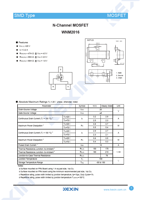
FEATURES
● VDS (V) =20 V● ID = 3.2 A
● RDS(ON) < 47m Ω @ VGS = 4.5 V
● RDS(ON) < 55m Ω @ VGS = 2.5 V
● RDS(ON) < 66m Ω @ VGS = 1.8 V D +0.1 2.4 -0.1 SOT-23 2.9 +0.1 -0.1 0.4 +0.1 -0.1 3 1 2 0.95 +0.1 -0.1 1.9 +0.1 -0.1 +0.1 1.3 -0.1 +0.1 0.97 -0.1 0.55 0.4 Unit : mm 0.1 +0.05 -0.01 1. Gate 2. Source 3. Drain 0-0.1 +0.1 0.38 -0.1 G S
●
ABSOLUTE MAXIMUM RATINGS
TA = 25℃ unless otherwise noted Parameter Symbol 10 S Steady State Drain-Source Voltage VDS 20 Gate-Source Voltage VGS ±8 Continuous Drain Current (TJ = 150 °C) a TA=25℃ ID TA=70℃ 3.2 2.9 2.5 2.3 Maximum Power Dissipation a TA=25℃ 0.8 0.7 PD TA=70℃ 0.5 0.4 Continuous Drain Current (TJ = 150 °C) b TA=25℃ ID TA=70℃ 2.9 2.7 2.3 2.1 Maximum Power Dissipation b Pulsed Drain Current c Thermal Resistance.Junction- to-Ambient a Thermal Resistance.Junction- to-Ambient b TA=25℃ TA=70℃ PD IDM RthJA RthJA 0.6 0.5 0.4 0.3 10 150 175 180 210 Junction-to-Case Thermal Resistance RthJC 76 Junction Temperature TJ 150 Storage Temperature Range Tstg...
