Datasheet Summary
Memory Module Specifications
KVR1333D3S8N9/2G
2GB 1Rx8 256M x 64-Bit PC3-10600 CL9 240-Pin DIMM
Important Information: The module defined in this data sheet is one of several configurations available under this part number. While all configurations are patible, the DRAM bination and/or the module height may vary from what is described here.
DESCRIPTION
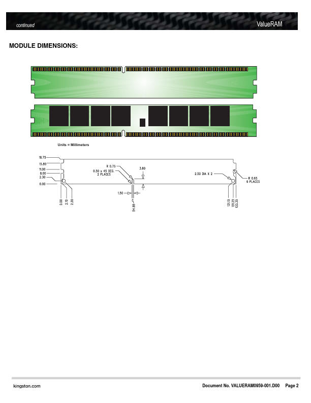
This document describes ValueRAM's 256M x 64-bit (2GB) DDR3-1333 CL9 SDRAM (Synchronous DRAM), 1Rx8 memory module, based on eight 256M x 8-bit DDR3-1333 FBGA ponents. The SPD is programmed to JEDEC standard latency DDR3-1333 timing of 9-9-9 at 1.5V. This 240-pin DIMM uses gold contact fingers. The electrical and mechanical...