ML145146
ML145146 is 4-Bit Data Bus Input PLL Frequency Synthesizer manufactured by LANSDALE Semiconductor.
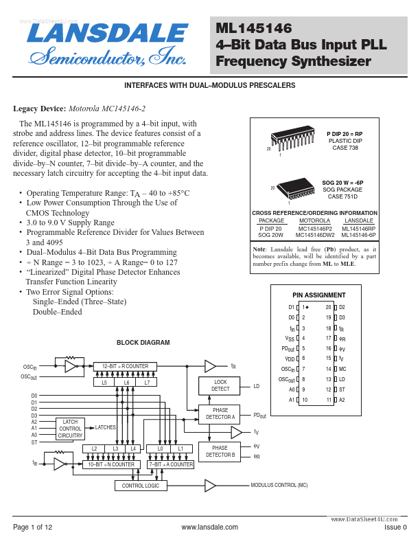
features consist of a reference oscillator, 12- bit programmable reference divider, digital phase detector, 10- bit programmable divide- by- N counter, 7- bit divide- by- A counter, and the necessary latch circuitry for accepting the 4- bit input data.
- Operating Temperature Range: TA
- 40 to +85°C
- Low Power Consumption Through the Use of CMOS Technology
- 3.0 to 9.0 V Supply Range
- Programmable Reference Divider for Values Between 3 and 4095
- Dual- Modulus 4- Bit Data Bus Programming
- ÷ N Range = 3 to 1023, ÷ A Range= 0 to 127
- “Linearized” Digital Phase Detector Enhances Transfer Function Linearity
- Two Error Signal Options: Single- Ended (Three- State) Double- Ended
P DIP 20 = RP PLASTIC DIP CASE 738
SOG 20 W = -6P SOG PACKAGE CASE 751D
CROSS REFERENCE/ORDERING INFORMATION PACKAGE MOTOROLA LANSDALE P DIP 20 MC145146P2 ML145146RP SOG 20W MC145146DW2 ML145146-6P
Note: Lansdale lead free (Pb) product, as it bees available, will be identified by a part number prefix change from ML to MLE.
PIN ASSIGNMENT
D1 D0 fin 1 2 3 4 5 6 7 8 9 10 20 19 18 17 16 15 14 13 12 11 D2 D3 f R φR φV f V MC LD ST A2
BLOCK DIAGRAM
VSS PDout
OSCin OSCout D0 D1 D2 D3 A2 A1 A0 ST
12- BIT ÷ R COUNTER L5 L6 L7 LOCK DETECT
VDD f R OSCin OSCout LD A0 A1 PHASE DETECTOR A PDout f V
LATCH CONTROL CIRCUITRY
LATCHES
L2 fin
L3
L4
L0
L1
PHASE DETECTOR B
φV φR
10- BIT ÷ N COUNTER
7- BIT ÷ A COUNTER
CONTROL LOGIC
MODULUS CONTROL (MC)
Page 1 of...