ML145428
ML145428 is Asynchronous-to-Synchronous and Synchronous-to-Asynchronous Converter manufactured by LANSDALE Semiconductor.
..
Asynchronous- to- Synchronous and Synchronous- to- Asynchronous Converter
Legacy Device: Motorola MC145428
The ML145428 Data Set Interface provides asynchronous-to-synchronous and synchronous-to-asynchronous data conversion. It is ideally suited for voice/data digital telesets supplying an EIA-232 patible data port into a synchronous transmission link. Other applications include: data multiplexers, concentrators, data-only switching, and PBX-based local area networks. This low-power CMOS device directly interfaces with either the 64 kbps or 8kbps channel of Motorola’s MC145422 and MC145426 Universal Digital Loop Transceivers (UDLTs), as well as the MC145421 and MC145425 Second Generation Universal Digital Loop Transceivers (UDLT II).
- Provides the Interface Between Asynchronous Data Ports and Synchronous Transmission Lines
- Up to 128 kbps Asynchronous Data Rate Operation
- Up to 2.1 Mbps Synchronous Data Rate Operation
- On-Board Bit Rate Clock Generator with Pin Selectable Bit Rates of 300, 1200, 1400, 4800, 9600, 19200 and 38400 bps or an Externally Supplied 16 Times Bit Rate Clock
- Accepts Asynchronous Data Words of 8 or 9 Bits in Length
- False Start Detection Provided
- Automatic Sync Insertion and Checking
- Single 5 V Power Supply
- Low Power Consumption of 5 m W Typical
- Application Notes AN943 and AN946
- Operating Temperature Range TA =
- 40º to +85ºC.
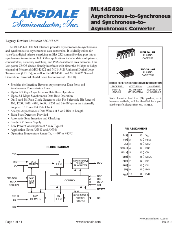
P DIP 20 = RP PLASTIC CASE 732
20 1
SOG 20 = -6P PLASTIC CASE 751D
CROSS REFERENCE/ORDERING INFORMATION MOTOROLA LANSDALE PACKAGE P DIP 20 MC145428P ML145428RP SOG 20 MC145428DW ML145428-6P
Note: Lansdale lead free (Pb) product, as it bees available, will be identified by a part number prefix change from ML to MLE.
PIN ASSIGNMENT
Tx S Tx D DL 1 2 3 20 19 18 17 16 15 14 13 12 11 VDD RESET DCO DOE CM DCLK DIE DCI Rx S Rx D
BLOCK DIAGRAM
Tx S Tx D DL DATA STRIPPER Tx FIFO SYNCHRONOUS CHANNEL TRANSMITTER DCO
BRCLK 4 BCLK 5 BR1 6 BR2 7 BR3 8 SB 9 10 VSS
BR1-BR3 BCLK BRCLK
BAUD RATE...