LS7211N
LS7211N is PROGRAMMABLE DIGITAL DELAY TIMER manufactured by LSI.
FEATURES
:
- 8-bit programmable delay from microseconds to days
- On chip oscillator (RC or Crystal) or external clock time base
- Selectable prescaler for real time delay generation based on 50Hz/60Hz time base or 32,768Hz watch crystal
- Four operating modes
- Reset input for delay abort
- Low quiescent and operating current
- Direct relay drive
- +3V to +18V operation (VDD
- VSS)
- LS7211N, LS7212N (DIP); LS7211N-S, LS7212N-S (SOIC)
- See Figure 1 DESCRIPTION
: The LS7211N and LS7212N are CMOS integrated circuits for generating digitally programmable delays. The delay is controlled by 8 binary weighted inputs, WB0
- WB7, in conjunction with an applied clock or oscillator frequency. The programmed time delay manifests itself in the Delay Output (OUT) as a function of the Operating Mode selected by the Mode Select inputs A and B: One-Shot, Delayed Operate, Delayed Release or Dual Delay. The time delay is initiated by a transition of the Trigger Input (TRIG).
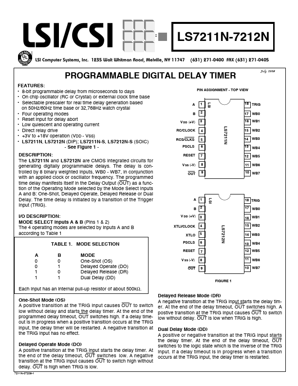
PIN ASSIGNMENT
- TOP VIEW
A1
B V DD (+V)
2 3
RC/CLOCK 4
RCS/CLKS PSCLS
5 6
RESET 7
V SS (-V) OUT
8 9
18 TRIG
17 WB0 16 WB1
15 WB2 14 WB3 13 WB4 12 WB5 11 WB6 10 WB7
A1 B2
18 TRIG 17 WB0
LS7212N
I/O DESCRIPTION
: MODE SELECT Inputs A & B (Pins 1 & 2) The 4 operating modes are selected by Inputs A and B according to Table 1
V DD (+V) 3
XTLI/CLOCK XTLO
4 5
16 WB1 15 WB2 14 WB3
TABLE 1. MODE SELECTION A B MODE 0 0 One-Shot (OS) 0 1 Delayed Operate (DO) 1 0 Delayed Release (DR) 1 1 Dual Delay...