Lattice Semiconductor 3256A
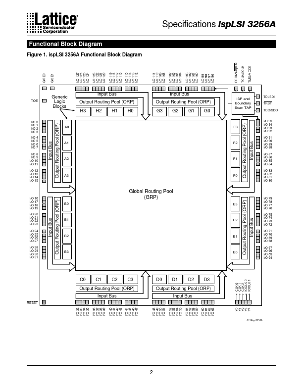
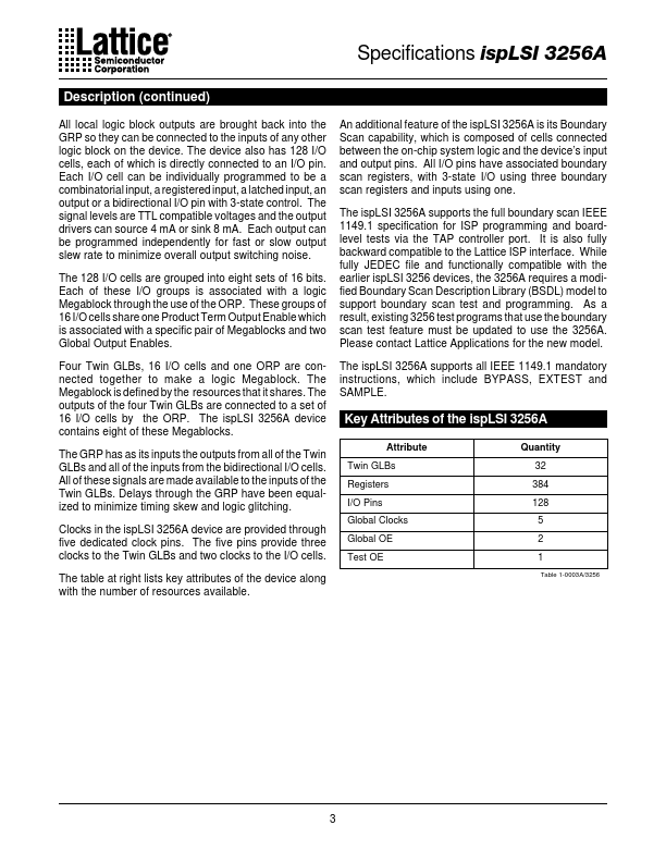
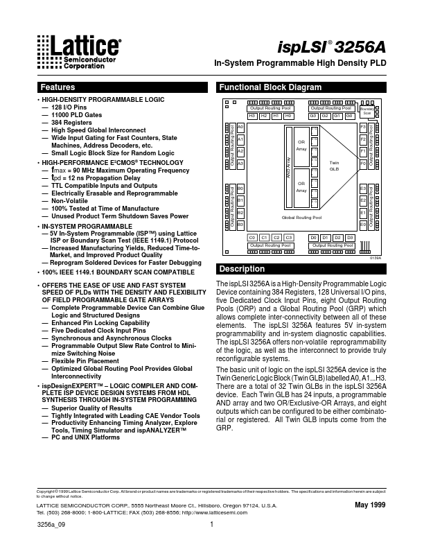
3256A is a High-Density Programmable Logic Device containing 384 Registers, 128 Universal I/O pins, five Dedicated Clock Input Pins, eight Output Routing Pools (ORP) and a Global Routing Pool (GRP) which allows complete inter-connectivity between all of these elements. The ispLSI 3256A features 5V in-system programmability and in-system diagnostic capabilities. The ispLSI 3256A offers non-volatile reprogrammability of the logic, as well as the interconnect to provide truly reconfigurable systems.| Part No. | 3256A |
|---|---|
| Datasheet | 3256A Download |
| Manufacturer |  Lattice Semiconductor |
| Description | In-System Programmable High Density PLD |
| Buy | Stock & Price |
FEATURES
● HIGH-DENSITY PROGRAMMABLE LOGIC — 128 I/O Pins — 11000 PLD Gates — 384 Registers — High Speed Global Interconnect — Wide Input Gating for Fast Counters, State Machines, Address Decoders, etc. — Small Logic Block Size for Random Logic● HIGH-PERFORMANCE E CMOS TECHNOLOGY — fmax = 90 MHz Maximum Operating Frequency — tpd = 12 ns Propagation Delay — TTL Compatible Inputs and Outputs — Electrically Erasable and Reprogrammable — Non-Volatile — 100% Tested at Time of Manufacture — Unused Product Term Shutdown Saves Power
● IN-SYSTEM PROGRAMMABLE — 5V In-System Programmable (ISP™) using Lattice ISP or Boundary Scan Test (IEEE 1149.1) Protocol — Increased Manufacturing Yields, Reduced Time-toMarket, and Improved Product Quality — Reprogram Soldered Devices for Faster Debugging
● 100% IEEE 1149.1 BOUNDARY SCAN COMPATIBLE
● OFFERS THE EASE OF USE AND FAST SYSTEM SPEED OF PLDs WITH THE DENSITY AND FLEXIBILITY OF FIELD PROGRAMMABLE GATE ARRAYS — Complete Programmable Device Can Combine...