Datasheet4U Logo Datasheet4U.com

OR2C15A - Field-Programmable Gate Arrays

Datasheet Summary

Description

3 ispLEVER Development System Overview 7 Architecture 7 Programmable Logic Cells 7 Programmable Function Unit 7 Look-Up Table Operating Modes 9 Latches/Flip-Flops 17 PLC Routing Resources 19 PLC Architectural Description 24 Programmable Input/Output Cells 27 Inputs 27 Outputs 28 5 V Tolerant I/O (OR

Features

  • High-performance, cost-effective, low-power 0.35 µm CMOS technology (OR2CxxA), 0.3 µm CMOS technology (OR2TxxA), and 0.25 µm CMOS technology (OR2TxxB), (four-input look-up table (LUT) delay less than 1.0 ns with -8 speed grade) High density (up to 43,200 usable, logic-only gates; or 99,400 gates including RAM) Up to 480 user I/Os (OR2TxxA and OR2TxxB I/Os are 5 V tolerant to allow interconnection to both 3.3 V and 5 V de.

📥 Download Datasheet

Datasheet preview – OR2C15A

Datasheet Details

Part number OR2C15A
Manufacturer Lattice
File Size 3.12 MB
Description Field-Programmable Gate Arrays
Datasheet download datasheet OR2C15A Datasheet
Additional preview pages of the OR2C15A datasheet.
Other Datasheets by Lattice

Full PDF Text Transcription

Click to expand full text
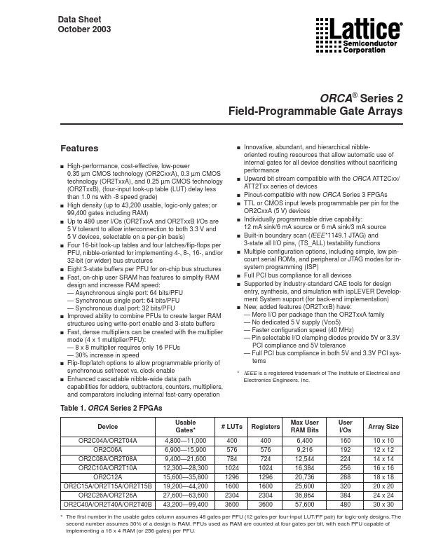
Data Sheet October 2003 ORCA® Series 2 Field-Programmable Gate Arrays Features ■ ■ ■ ■ ■ ■ ■ ■ ■ ■ ■ High-performance, cost-effective, low-power 0.35 µm CMOS technology (OR2CxxA), 0.3 µm CMOS technology (OR2TxxA), and 0.25 µm CMOS technology (OR2TxxB), (four-input look-up table (LUT) delay less than 1.0 ns with -8 speed grade) High density (up to 43,200 usable, logic-only gates; or 99,400 gates including RAM) Up to 480 user I/Os (OR2TxxA and OR2TxxB I/Os are 5 V tolerant to allow interconnection to both 3.
Published: |