LTC6601-1
Key Features
- n n n n
- LTC6601-1 Low Noise, 0.5% Tolerance, 5MHz to 28MHz, Pin Configurable Filter/ADC Driver DESCRIPTION n n n
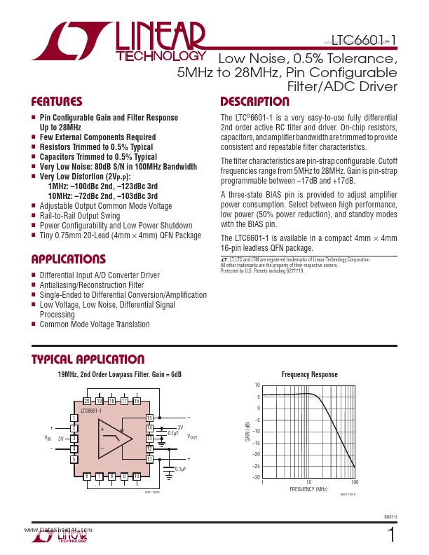
- Pin Configurable Gain and Filter Response Up to 28MHz Few External Components Required Resistors Trimmed to 0.5% Typical Capacitors Trimmed to 0.5% Typical Very Low Noise: 80dB S/N in 100MHz Bandwidth Very Low Distortion (2VP-P): 1MHz: -100dBc 2nd, -123dBc 3rd 10MHz: -72dBc 2nd, -103dBc 3rd Adjustable Output Common Mode Voltage Rail-to-Rail Output Swing Power Configurability and Low Power Shutdown Tiny 0.75mm 20-Lead (4mm × 4mm) QFN Package The LTC®6601-1 is a very easy-to-use fully differential 2nd order active RC filter and driver. On-chip resistors, capacitors, and amplifier bandwidth are trimmed to provide consistent and repeatable filter characteristics. The filter characteristics are pin-strap configurable. Cutoff frequencies range from 5MHz to 28MHz. Gain is pin-strap programmable between -17dB and +17dB. A three-state BIAS pin is provided to adjust amplifier power consumption. Select between high performance, low power (50% power reduction), and standby modes with the BIAS pin. The LTC6601-1 is available in a compact 4mm × 4mm 16-pin leadless QFN package.