LTC6957-1
Overview
- Low Phase Noise Buffer/Driver
- Optimized Conversion of Sine Wave Signals to Logic Levels
- Three Logic Output Types Available - LVPECL - LVDS - CMOS
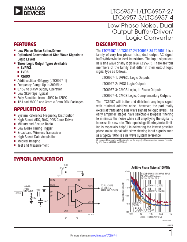
- Additive Jitter 45fsRMS (LTC6957-1)
- Frequency Range Up to 300MHz
- 3.15V to 3.45V Supply Operation
- Low Skew 3ps Typical
- Fully Specified from -40°C to 125°C
- 12-Lead MSOP and 3mm × 3mm DFN Packages