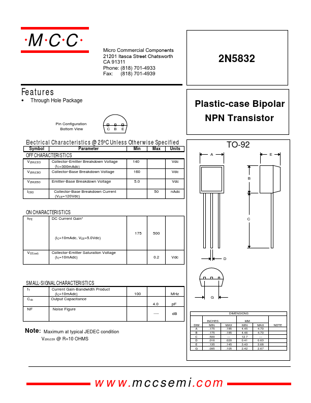
● Through Hole Package omponents 21201 Itasca Street Chatsworth ! "# $ % ! "# 2N5832 Plastic-case Bipolar NPN Transistor C B E Pin Configuration Bottom View
ELECTRICAL CHARACTERISTICS
@ 25°C Unless Otherwise Specified Symbol Parameter Collector-Emitter Breakdown Voltage (I C=300mAdc) Collector-Base Breakdown Voltage Emitter-Base Breakdown Voltage Collector-Base Breakdown Current (VCE=120Vdc) Min 140 160 5.0 50 Max Units A Vdc Vdc Vdc nAdc TO-92 E OFF CHARACTERISTICS V(BR)CEO V(BR)CBO V(BR)EBO ICBO B ON CHARACTERISTICS hFE DC Current Gain* C 175 (I C=10mAdc, VCE=5.0Vdc) 500 VCE(sat) Collector-Emitter Saturation Voltage (I C=10mAdc) 0.2 Vdc D SMALL-SIGNAL CHARACTERISTICS fT Cob NF Current Gain-Bandwidth Product (I C=10mAdc) Output Capacitance Noise Figure ---dB DIM A B C D E G INCHES MIN .175 .175 .500 .016 .135 .095 DIMENSIONS MM MIN 4.45 4.46 12.7 0.41 3.43 2.42 100 4.0 MHz pF G Note: Maximum at typical JEDEC condition V(BR)CER @ R=10 OHMS MAX .185 .185 --.020 .145 .105 MAX 4.
This website uses cookies or similar technologies, to enhance your browsing experience and provide personalized recommendations. By continuing to use our website, you agree to our Privacy Policy