SeCoS Halbleitertechnologie GmbH 2N5832
NPN Plastic Encapsulated Transistor
| Part No. | 2N5832 |
|---|---|
| Datasheet | 2N5832 Download |
| Manufacturer |  SeCoS Halbleitertechnologie GmbH |
| Description | NPN Plastic Encapsulated Transistor |
| Buy | Stock & Price |
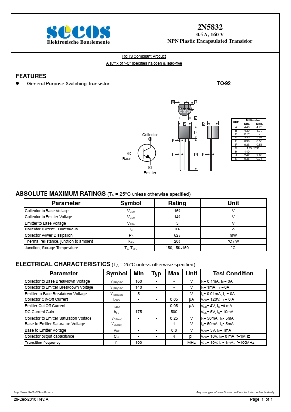
FEATURES
● General Purpose Switching Transistor TO-92 Collector● Base Emitter GH J AD B K E CF REF. A B C D E F G H J K Millimeter Min. Max. 4.40 4.70 4.30 4.70 12.70 - 3.30 3.81 0.36 0.56 0.36 0.51 1.27 TYP. 1.10 - 2.42 2.66 0.36 0.76