Micro Commercial Components SI2301
P-Channel Enhancement Mode Field Effect Transistor
| Part No. | SI2301 |
|---|---|
| Datasheet | SI2301 Download |
| Manufacturer |  Micro Commercial Components |
| Description | P-Channel Enhancement Mode Field Effect Transistor |
| Buy | Stock & Price |
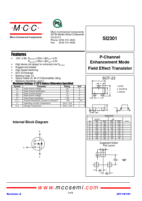
FEATURES
●●
●
●
●
●
●
●
MAXIMUM RATINGS
@ 25OC Unless Otherwise Specified Symbol VDS ID IDM VGS PD RθJA TJ TSTG Parameter Drain-source Voltage Drain Current-Continuous Drain Current-Pulsed a Gate-source Voltage Total Power Dissipation Thermal Resistance Junction to Ambientb Operating Junction Temperature Storage Temperature Rating -20 -2.8 -10 ±8 1.25 100 -55 to +150 -55 to +150 Unit V A A V W ℃/W ℃ ℃ -20V,-2.8A, RDS(ON)=120mΩ@VGS=-4.5V RDS(ON)=150mΩ@VGS=-2.5V High dense cell design for extremely low RDS(ON) Rugged and reliable High Speed Switching SOT-23 Package Marking Code: S1 Epoxy meets UL 94 V-0 flammability rating Moisture Sensitivity Level 1 P-Channel Enhancement Mode Field Effect Transistor SOT-23 A D 3 1.GATE C B 2. SOURCE 3. DRAIN 1 F E 2 G K H J DIMENSIONS INCHES MIN .110 .083 .047 .035 .070 .018 .0005 .035 .003 .015 MM MIN 2.80 2.10 1.20 .89 1.78 .45 .013 .89 .085 .37 Internal Block Diagram D DIM A B C D E F G H J K MAX .120 .098 .055 .041 .081 .024 .0039 .044 .007 .020 M...