Si2301
Description
Si2301 P-Channel Enhancement Mode Field Effect Transistor FEATURES Super high dense cell design for low RDS(ON) Rugged and reliable Simple drive requirement SOT-23 package PRODUCT SUMMARY VDSS ID...
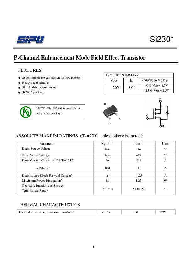
Si2301 P-Channel Enhancement Mode Field Effect Transistor FEATURES Super high dense cell design for low RDS(ON) Rugged and reliable Simple drive requirement SOT-23 package PRODUCT SUMMARY VDSS ID...
| Part Number | Manufacturer | Description |
|---|---|---|
| Si2301DS | TEMIC Semiconductors | P-Channel MOSFET |
| SI2306 | Micro Commercial Components | N-Channel Enhancement Mode Field Effect Transistor |
| SI2300 | Micro Commercial Components | N-Channel MOSFET |
| SI2304 | Micro Commercial Components | N-channel FET |
| SI2304 | PUOLOP | 30V N-Channel Enhancement Mode MOSFET |
| SI2305 | HT Semi | 20V P-Channel MOSFET |
| SI2303 | Micro Commercial Components | P-Channel Enhancement Mode Field Effect Transistor |
| Si2303 | Tuofeng | P-Channel MOSFET |
| SI2303DS-HF | Kexin Semiconductor | P-Channel MOSFET |
| SI2302S | Meitai Microelectronics | 20V N-Channel MOSFET |