MM3474L02VBE Overview
Description
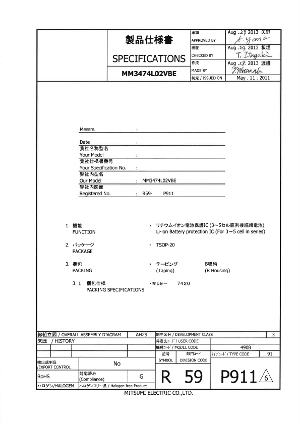
TSOP-20Cパッケージ 5 Package type of T.
| Part | MM3474L02VBE |
|---|---|
| Description | Li-ion battery protection |
| Manufacturer | MITSUMI |
| Size | 492.65 KB |
TSOP-20Cパッケージ 5 Package type of T.
| Part Number | Manufacturer | Description |
|---|---|---|
| CM1051 | iCM | 5-series rechargeable lithium battery protection |
| CW1073 | Cellwise | 6-7 Battery protection |
| CW1244 | Cellwise | Li-Ion/Polymer Battery Pack Protection IC |