2SD1815
Features
- Low Collector-to-Emitter Saturation Voltage
- Excllent Linearity of h FE
- High f T
- Fast Switching Time
Transistors(NPN)
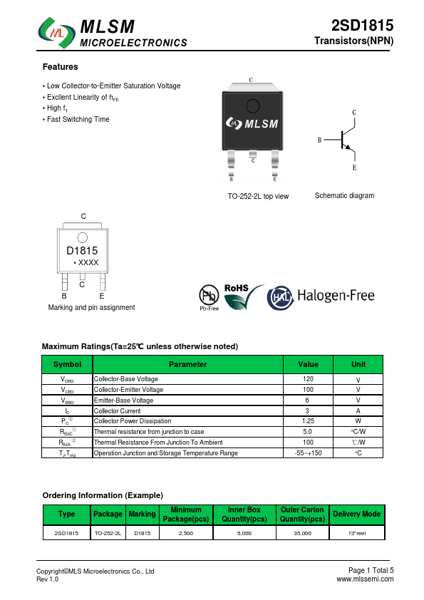
D1815
- XXXX
Marking and pin assignment
TO-252-2L top view
Schematic diagram
Maximum Ratings(Ta=25℃ unless otherwise noted)
Symbol
VCBO VCEO VEBO
IC PC② RΘJC① RθJA ② TJ,Tstg
Parameter
Collector-Base Voltage Collector-Emitter Voltage Emitter-Base Voltage Collector Current Collector Power Dissipation Thermal resistance from junction to case Thermal Resistance From Junction To Ambient Operation Junction and Storage Temperature Range
Value
120 100 6 3 1.25 5.0 100 -55~+150
Unit
V V V A W °C/W ℃/W °C
Ordering Information (Example)
Type
Package
Marking
Minimum Package(pcs)
TO-252-2L D1815
2,500
Inner Box Quantity(pcs)
5,000
Outer Carton Quantity(pcs)
Delivery Mode
35,000
13"reel
Copyright©MLS Microelectronics Co., Ltd Rev 1.0
Page 1 Total 5...