MMBD4448DW
Features
- Fast switching speed
- Ultra-Small Surface Mount Package
- For general purpose switching applications
- High Conductance Power Dissipation
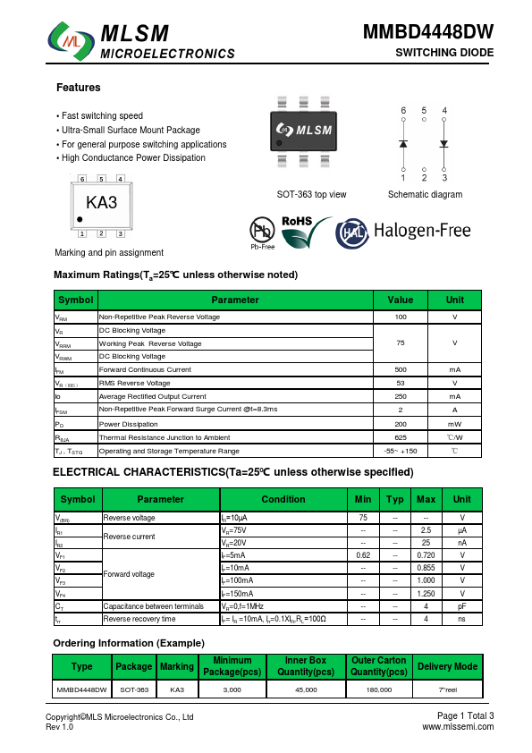
KA3
SWITCHING DIODE
SOT-363 top view
Schematic diagram
Marking and pin assignment
Maximum Ratings(Ta=25℃ unless otherwise noted)
Symbol
Parameter
VRM VR VRRM VRWM IFM VR(RMS) Io IFSM PD RθJA TJ , TSTG
Non-Repetitive Peak Reverse Voltage DC Blocking Voltage Working Peak Reverse Voltage DC Blocking Voltage Forward Continuous Current RMS Reverse Voltage Average Rectified Output Current Non-Repetitive Peak Forward Surge Current @t=8.3ms Power Dissipation Thermal Resistance Junction to Ambient Operating and Storage Temperature Range
Value
500 53 250 2 200 625 -55~ +150
ELECTRICAL CHARACTERISTICS(Ta=25℃ unless otherwise specified)
Unit
V m A V m A A m W ℃/W ℃
Symbol
Parameter
V(BR)
Reverse voltage
IR1
Reverse current
IR2
VF1
VF2
Forward voltage
VF3
VF4
Capacitance between terminals trr
Reverse...