MSP0307W
Features
- VDS =-30V,ID =-6.5A RDS(ON) < 42mΩ @ VGS=-10V RDS(ON) < 72mΩ @ VGS=-4.5V
- High density cell design for ultra low Rdson
- Fully characterized avalanche voltage and current
Application
- Load switch
- battery protection
Lead Free
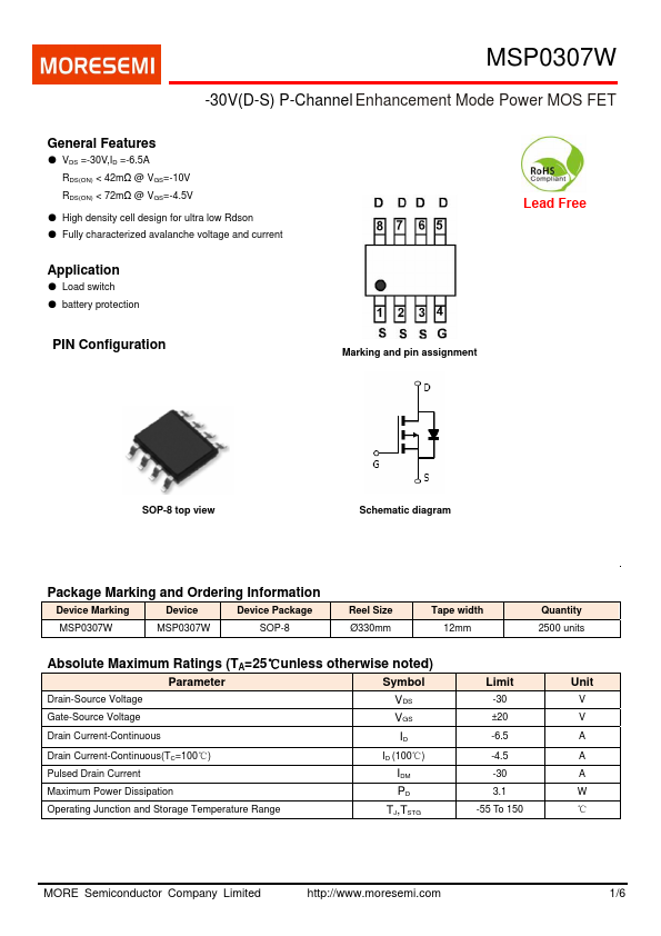
PIN Configuration
Marking and pin assignment
SOP-8 top view
Schematic diagram
Package Marking and Ordering Information
Device Marking
Device
Device Package
SOP-8
Reel Size Ø330mm
Tape width 12mm
Quantity 2500 units
Absolute Maximum Ratings (TA=25℃unless otherwise noted)
Parameter
Symbol
Drain-Source Voltage
Gate-Source Voltage
Drain Current-Continuous
Drain Current-Continuous(TC=100℃)
ID (100℃)
Pulsed Drain Current Maximum Power Dissipation Operating Junction and Storage Temperature Range
IDM PD TJ,TSTG
Limit
-30 ±20 -6.5 -4.5 -30 3.1 -55 To 150
Unit
V V A A A W ℃
MORE Semiconductor pany...