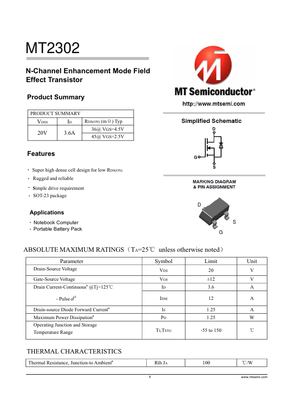
MT2302
Features
Super high dense cell design for low RDS(ON) Rugged and reliable Simple drive requirement SOT-23 package
$SSOLFDWLRQV
Notebook puter Portable Battery Pack
ABSOLUTE MAXIMUM RATINGS˄TA=25ć unless otherwise noted˅
Parameter
Drain-Source Voltage
Gate-Source Voltage Drain Current-Continuous嘌@Tj=125ć
Symbol
VDS VGS ID
Limit
Unit
±12
- Pulse d b
Drain-source Diode Forward Current嘌 Maximum Power Dissipation嘌 Operating Junction and Storage Temperature Range
IS PD
TJ,TSTG
-55 to 150
ć
THERMAL CHARACTERISTICS
Thermal Resistance, Junction-to Ambient嘌
Rth JA
ć/W
ZZZPWVHPLFRP
ELECTRICAL CHARACTERISTICS (TA=25ć unless otherwise noted)
Parameter
OFF CHARACTERISTICS Drain-Source Breakdown Voltage Zero Gate Voltage Drain Current Gate-Body Leakage
ON CHARACTERITICS
Gate Threshold Voltage
Drain-Source On-State Resistance
Forward Transconductance DYNAMIC CHARACTERISTICS Input Capacitance...