Datasheet Summary
..
8M-BIT MASK ROM (8/16 BIT OUTPUT)
Features
- Bit organization
- 1M x 8 (byte mode)
- 512K x 16 (word mode)
- Fast access time
- Random access: 95ns (max.)
- Page access: 50ns (max.)
- Current
- Operating: 60mA
- Standby: 100uA
- Supply voltage
- 5V±10%
- Package
- 44 pin SOP (500mil)
- 42 pin PDIP (600mil)
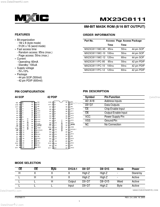
ORDER INFORMATION
Part No. Access Page Access Package Time MX23C8111MC-95 95ns Time 50ns 50ns 60ns 50ns 50ns 60ns 44 pin SOP 44 pin SOP 44 pin SOP 42 pin PDIP 42 pin PDIP 42 pin PDIP
MX23C8111MC-10 100ns MX23C8111MC-12 120ns MX23C8111PC-95 95ns
MX23C8111PC-10 100ns MX23C8111PC-12 120ns
PIN CONFIGURATION
44 SOP
NC A18 A17 A7 A6 A5 A4 A3 A2 A1 A0 CE VSS...