Datasheet Summary
..
512M-BIT (16M x 32) MASK ROM WITH PAGE MODE (SSOP ONLY)
Features
- Bit organization
- 16M x 32 (double word mode) only
- Fast access time
- Random access: 90ns (max.)
- Page access: 30ns (max.)
- Page size
- 8 double words per page
- Current
- Operating: 80mA (max.) @ 5MHz
- Standby: 30uA (max.)
- Supply voltage : 3.3V ± 10%
- Package
- 70 pin SSOP
- Temperature
- 0~70° C
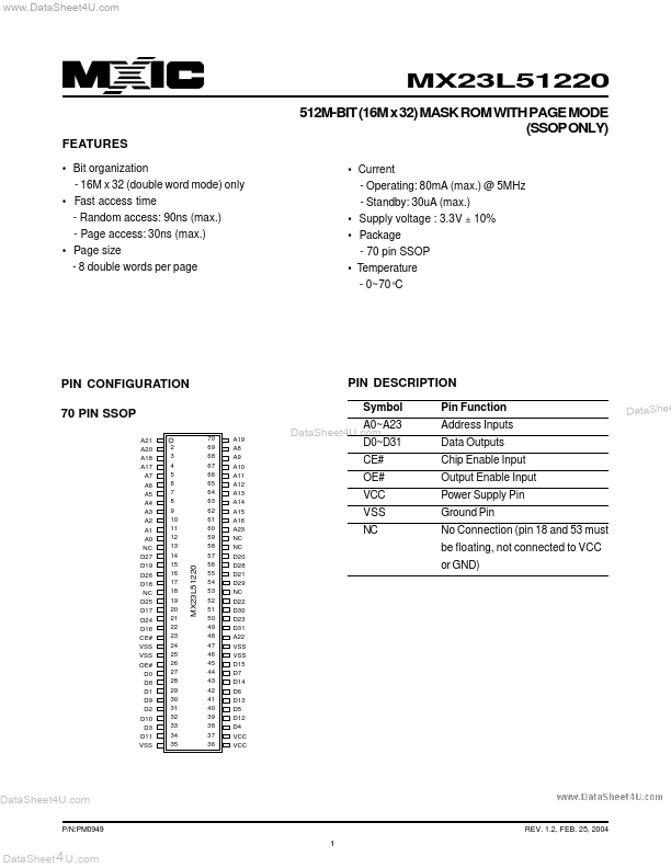
PIN CONFIGURATION 70 PIN SSOP
A21 A20 A18 A17 A7 A6 A5 A4 A3 A2 A1 A0 NC D27 D19 D26 D18 NC D25 D17 D24 D16 CE# VSS VSS OE# D0 D8 D1 D9 D2 D10 D3 D11 VSS 2 3 4 5 6 7 8 9 10 11 12 13 14 15 16 17 18 19 20 21 22 23 24 25 26 27 28 29 30 31 32 33 34 35 70 69 68 67 66 65 64 63 62 61 60 59 58 57...